
 My Inquiry
 My Account


Winbond Electronics Corporation W957D8MFYA5I TR
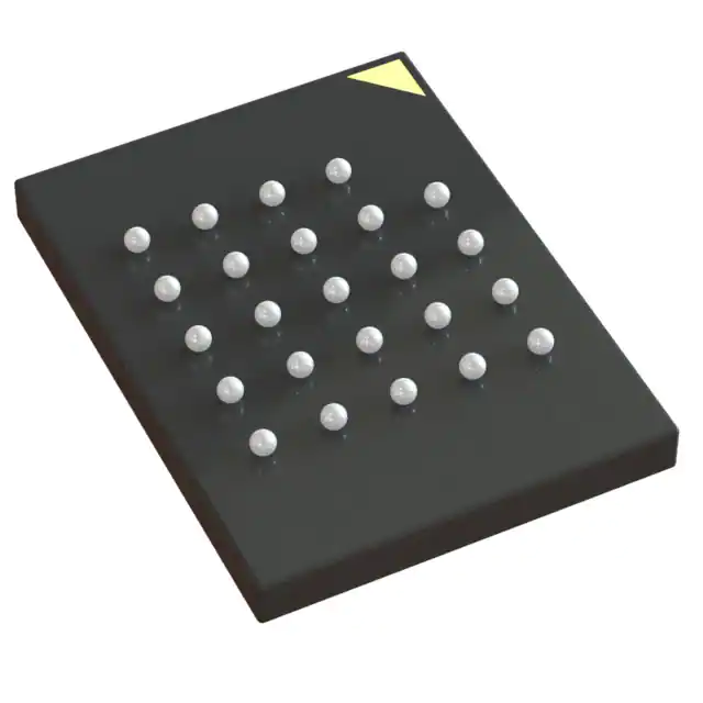
- Part No.:
- W957D8MFYA5I TR
- Manufacturer:
- Winbond Electronics Corporation
- Category:
- Memory
- Package:
- 24-TBGA
- Datasheet:
-
 W957D8MFYA5I TR.pdf
- Description:
- IC DRAM 128MBIT HYPERBUS 24TFBGA
- Quantity:
- Payment:

- Shipping:

Inventory:1,819
Please send an inquiry. Send us your inquiry, and we will respond immediately.
Product details
Overview
W957D8MFYA5I from Winbond Electronics is a 128Mb (16MB) HyperRAM device operating at 1.8V, featuring a DDR HyperBus interface with 200MHz clock support and up to 400 MT/s data throughput. It implements Dual-Die-Package (DDP) architecture in a 24-ball TFBGA, enabling high-bandwidth, low-pin-count memory expansion for microcontroller-based graphics and real-time control systems.
For engineers reviewing the W957D8MFYA5I datasheet, W957D8MFYA5I pinout, W957D8MFYA5I application, or W957D8MFYA5I equivalent, key selection considerations include its configurable burst modes (wrapped/linear/hybrid), dual-die addressing, RWDS-synchronized read/write timing, and support for Hybrid Sleep and Deep Power Down modes in industrial temperature range (-40°C to +85°C).
Technical Context
The W957D8MFYA5I uses a DDR HyperBus interface with differential (CK/CK#) or single-ended (CK only) clocking, where all command/address/data transfers occur on the 8-bit DQ[7:0] bus using center-aligned CA and edge-aligned read data. RWDS serves as bidirectional strobe/mask-output during CA phase to signal refresh latency, output as read data strobe, and input as write mask.
Internally, it integrates two 64Mb dies in one package, supporting die-selectable addressing and boundary-crossing burst operations. Configuration registers enable runtime control of initial/fixed latency, drive strength, partial array refresh, and hybrid sleep entry/exit timing-all accessible via HyperBus register space without requiring external configuration pins.
Key Specifications
| Parameter | Value and Actual Design Meaning |
|---|---|
| Memory Density | 128Mb (16MB) total capacity across two 64Mb dies in DDP configuration |
| Interface | HyperBus DDR: 8-bit DQ bus + CK/CK# or CK-only clock + CS# + RWDS + RESET# |
| Max Clock Rate | 200MHz - enables sustained 400 MB/s read throughput (1B × 2 edges × 200MHz) |
| Supply Voltage | VCC/VCCQ = 1.7V–2.0V - supports low-power SoC integration with separate I/O and core rails |
| Operating Temp | -40°C to +85°C case temperature - qualified for industrial embedded applications |
| Burst Modes | Configurable wrapped (16/32/64/128-byte), linear, or hybrid burst - optimizes cache-line fill vs. sequential streaming |
| Power Modes | Hybrid Sleep (fast wake) and Deep Power Down (ultra-low ICC) - reduces system standby power |
Pinout & Package
W957D8MFYA5I is housed in a 24-ball Thin Fine-Pitch Ball Grid Array (TFBGA) package with 5×5 mm footprint and 0.5 mm ball pitch. The Dual-Die-Package (DDP) integrates two identical 64Mb HyperRAM dies sharing all interface signals except internal die-select logic.
| Pin/Terminal | Circuit Role | Design Meaning |
|---|---|---|
| CS# | Input | Active-low chip select initiating all HyperBus transactions; deassertion terminates transfer |
| CK / CK# | Input | Differential clock pair (or CK-only mode); defines timing reference for CA and data capture |
| RWDS | Input/Output | Bidirectional strobe/mask: indicates initial latency during CA, acts as read strobe, and masks write bytes when high |
| RESET# | Input | Hardware reset with internal pull-up; forces device into Standby state and tri-states DQ/RWDS |
| DQ[7:0] | I/O | 8-bit bidirectional bus carrying command, address, and data; LV-CMOS compatible |
| VCC / VSS | Power | VCC powers core logic and input buffers; VSS is its ground reference |
| VCCQ / VSSQ | Power | VCCQ powers DQ and RWDS output drivers; VSSQ is its dedicated ground for noise isolation |
Key Features
| Feature | Design Value |
|---|---|
| HyperBus DDR Interface | Reduces pin count vs. parallel NOR/NAND while delivering 400 MB/s bandwidth via 8-bit bus and DDR clocking |
| Dual-Die-Package (DDP) | Integrates two 64Mb dies in one 24-ball TFBGA - doubles density without increasing PCB footprint or interface complexity |
| Configurable Burst Lengths | Supports 16/32/64/128-byte wrapped bursts and linear/hybrid modes - matches CPU cache line and framebuffer access patterns |
| Dynamic Latency Control | Initial and fixed latency settings adjustable per transaction - balances timing margin and throughput in mixed-workload systems |
| Partial Array Refresh | Refreshes only active memory regions - cuts refresh current by up to 50% versus full-array refresh during partial usage |
| Hybrid Sleep Mode | Enters low-power state in <1 µs with full retention; wakes in <50 ns - ideal for real-time interrupt-driven applications |
Applications
| Industrial HMI Displays | Automotive Digital Clusters |
|---|---|
Use Scenario: High-resolution TFT display buffering with real-time GUI updates and animation rendering. IC Role / Device Role / Timing Role: External frame buffer memory interfaced directly to MCU's HyperBus controller, providing low-latency pixel data access. Use Value: Linear burst mode delivers sustained 400 MB/s reads to feed 1080p@60Hz displays; Hybrid Sleep enables instant wake from idle without frame tearing. |
Use Scenario: Instrument cluster with safety-critical gauges, warning icons, and ADAS overlays requiring deterministic response. IC Role / Device Role / Timing Role: Dedicated memory for cluster MCU to store vector graphics assets and dynamic status data with guaranteed access timing. Use Value: Configurable initial latency and RWDS-synchronized reads ensure jitter-free rendering; -40°C to +85°C rating supports under-hood mounting. |
| Edge AI Inference Accelerators | Industrial PLC Motion Controllers |
Use Scenario: On-device neural network inference with weight caching and intermediate tensor storage. IC Role / Device Role / Timing Role: Off-chip memory supplementing limited on-die SRAM, accessed via burst-oriented HyperBus for weight matrix streaming. Use Value: Wrapped burst mode enables efficient cache-line-aligned weight fetches; Partial Array Refresh lowers average power during sparse inference workloads. |
Use Scenario: Real-time motion profiling with multi-axis interpolation, position lookup tables, and servo feedback buffering. IC Role / Device Role / Timing Role: High-speed memory for storing trajectory profiles and encoder history, accessed deterministically by motion engine. Use Value: 200MHz DDR interface meets sub-microsecond latency requirements; Deep Power Down reduces energy per motion cycle during dwell periods. |
Equivalent & Alternatives
The following parts are listed as comparable options for similar HyperRAM interface applications.
| Alternative Part | Technical Difference | Application Difference | Selection Advice |
|---|---|---|---|
| W957A8MFYA5I | 3.0V VCC/VCCQ supply; otherwise identical pinout, timing, and DDP architecture | Targets 3.3V legacy MCU platforms; incompatible with 1.8V-only SoCs | Select W957A8MFYA5I only when host system operates at 3.0V–3.6V and requires same 128Mb HyperRAM functionality. |
| IS66WV1288GBLL-150B3LI | Parallel async SRAM (128Mb, 15ns access); 48-pin TSOP-II; no HyperBus or power modes | Requires 28+ address + 8 data + control lines; higher pin count and static power draw | Choose only if HyperBus controller is unavailable and board layout allows wider bus; no power savings or burst optimization. |
Compared with W957A8MFYA5I, the W957D8MFYA5I enables lower system power and better noise immunity via 1.8V operation; compared with IS66WV1288GBLL-150B3LI, it reduces interface complexity by >60% pins and adds adaptive power management for battery-sensitive edge devices.
Availability
W957D8MFYA5I is available at Aetrix Electronics and suitable for industrial HMI displays, automotive digital clusters, edge AI accelerators, and industrial PLC motion controllers requiring stable component supply across extended temperature ranges and long production lifecycles.
Supply support for W957D8MFYA5I includes scheduled delivery planning, volume procurement assistance, BOM continuity management, traceable sourcing, and lifecycle availability coordination for OEM customers, industrial embedded developers, connected-device designers, and electronics production programs.
Manufacturer
Winbond Electronics is a Taiwan-based semiconductor company specializing in specialty memory solutions including SPI NOR Flash, WSON NAND, and high-performance RAM products for embedded and industrial markets.
The W957D8MFYA5I belongs to Winbond's HyperRAM family, designed specifically to replace parallel NOR/NAND and PSRAM in bandwidth-constrained, pin-limited microcontroller applications while maintaining deterministic timing and low power.
FAQ
What is the memory organization of the W957D8MFYA5I?
The W957D8MFYA5I contains two 64Mb dies in a Dual-Die-Package (DDP), totaling 128Mb (16MB) of memory. Each die is organized as 8,388,608 words × 16 bits, with addressing managed via HyperBus command/address protocol and die-select logic internal to the package. Row/column boundaries and burst alignment follow HyperBus specification v1.0.
Does the W957D8MFYA5I support both differential and single-ended clocking?
Yes, the W957D8MFYA5I supports both differential (CK/CK#) and single-ended (CK only) clocking modes. CK# is unused in single-ended mode, and the clock need not be free-running. This flexibility allows integration with MCUs offering either clock topology without external level-shifting or termination changes.
How does RWDS function during read and write operations in the W957D8MFYA5I?
In the W957D8MFYA5I, RWDS acts as an output during the Command/Address phase to indicate required refresh latency, as a read data strobe (edge-aligned with DQ) during read transfers, and as a write data mask (high = masked byte, low = valid byte) during write transfers. Its bidirectional behavior is intrinsic to HyperBus protocol and requires no mode pin.
What power-saving modes are implemented in the W957D8MFYA5I?
The W957D8MFYA5I implements Hybrid Sleep Mode (HSM) and Deep Power Down (DPD). HSM retains memory contents with sub-µs entry/exit and minimal current draw; DPD reduces ICC to ≤10 µA but requires longer wake time. Both are controlled via HyperBus configuration registers, enabling software-defined power policy.
Is the W957D8MFYA5I pin-compatible with other Winbond HyperRAM devices in the same package?
Yes, the W957D8MFYA5I shares identical 24-ball TFBGA pinout and ball assignment with W957A8MFYA5I and W957A8MFYA6I. All three support the same HyperBus interface signals (CS#, CK/CK#, RWDS, RESET#, DQ[7:0], VCC/VCCQ/VSS/VSSQ), enabling drop-in voltage-level replacement within the same PCB layout.
W957D8MFYA5I TR Specifications
- Product attributes
- Attribute value
- Manufacturer:
- Winbond Electronics Corporation
- Series:
- -
- Package/Case:
- 24-TBGA
- Packaging:
- Tape & Reel (TR)
- Product Status:
- Active
- Programmable:
- Not Verified
- Memory Type:
- Volatile
- Memory Format:
- DRAM
- Technology:
- HyperRAM
- Memory Size:
- 128Mbit
- Memory Organization:
- 16M x 8
- Memory Interface:
- HyperBus
- Clock Frequency:
- 200 MHz
- Write Cycle Time - Word, Page:
- 35ns
- Access Time:
- 36 ns
- Voltage - Supply:
- 3V ~ 3.6V
- Operating Temperature:
- -40°C ~ 85°C (TC)
- Grade:
- -
- Qualification:
- -
- Mounting Type:
- Surface Mount
- Supplier Device Package:
- 24-TFBGA, DDP (6x8)
W957D8MFYA5I TR FAQ
1.How can I place an order for W957D8MFYA5I TR through Aetrix?
Please submit a Request for Quotation (RFQ) for W957D8MFYA5I TR on Aetrix. Our sales agent will provide a competitive quotation and guide you through the order confirmation once you accept the terms.
2.Are the price and stock information for W957D8MFYA5I TR reliable?
The price and inventory of W957D8MFYA5I TR are updated periodically and may fluctuate due to market conditions. Stock and pricing data are typically refreshed every 24 hours. Quotation validity for W957D8MFYA5I TR is usually 5 days.
3.What payment methods are accepted for W957D8MFYA5I TR?
We accept Wire Transfer, PayPal, Credit Card, Western Union, MoneyGram, and Escrow for W957D8MFYA5I TR transactions.
Note: Certain payment methods may incur a processing fee.
4.How is shipping managed for W957D8MFYA5I TR?
W957D8MFYA5I TR orders can be shipped via leading logistics carriers, including DHL, UPS, FedEx, TNT, or Registered Mail.
Once your W957D8MFYA5I TR order is processed, you will receive an email with the shipment details and tracking number.
Note: Tracking information may take up to 24 hours to appear. Express delivery typically takes 3–5 business days.
5.How can I obtain technical support or documentation for W957D8MFYA5I TR?
For technical support, including W957D8MFYA5I TR datasheets, pinout diagrams, or application guidance, please contact our engineering support team. They can provide detailed documentation and assistance for your W957D8MFYA5I TR requirements.
6.How does Aetrix verify that W957D8MFYA5I TR is sourced from the original manufacturer or authorized distributors?
All W957D8MFYA5I TR products on Aetrix are procured from qualified distributors and authorized channels. Our dedicated quality assurance team conducts strict verification, including traceability checks and, if necessary, third-party testing. This ensures that W957D8MFYA5I TR meets industry standards.
7.What is the process for return or replacement of W957D8MFYA5I TR?
All W957D8MFYA5I TR units undergo pre-shipment inspection (PSI). If there is an issue with W957D8MFYA5I TR, returns or replacements are accepted under the following conditions:
1.Quantity discrepancies, incorrect items, or visible external defects (such as breakage or corrosion), acknowledged by Aetrix.
2.The issue is reported within 90 days of delivery.
3.The W957D8MFYA5I TR part is unused and in its original packaging.
Return procedure for W957D8MFYA5I TR:
1.Submit a request within 90 days.
2.Obtain a Return Material Authorization (RMA) from Aetrix.
W957D8MFYA5I TR Tags

-
M24C02-WMN6TP
STMicroelectronics

-
AT24C02C-XHM-T
Microchip Technology

-
AT21CS01-STUM10-T
Microchip Technology

-
AT24C02C-SSHM-T
Microchip Technology

-
24LC01BT-I/OT
Microchip Technology

-
M24C02-FMC6TG
STMicroelectronics
-
AT24CS02-SSHM-T
Microchip Technology

-
93LC46BT-I/OT
Microchip Technology
-
AT24C04C-SSHM-T
Microchip Technology

-
24LC01BT-I/SN
Microchip Technology
-
24AA02UIDT-I/OT
Microchip Technology

-
AT24C08C-STUM-T
Microchip Technology
Tech Hub

Counterfeit components can hide behind convincing markings and passing basic function tests. This engineering reference covers source traceability, external inspection, X-ray, XRF, electrical testing, …

A practical engineering and sourcing framework covering lifecycle verification, lifetime-buy calculations, replacement qualification, supplier checks and counterfeit-risk controls.

TTL and CMOS logic families differ in thresholds, loading, output drive, power and timing. This engineering guide compares 74HC and 74HCT, calculates noise margins and checks 3.3 V/5 V compatibility.

A practical engineering guide to 3.3V and 5V logic compatibility, input thresholds, resistor dividers, translator ICs, MOSFET level shifting, I2C pull-ups, timing limits and power-sequencing risks.

The 74HC595 uses push-pull logic outputs, while the TPIC6B595 uses 50 V open-drain DMOS sinks for higher-power loads. This guide compares timing, current limits, 3.3 V interfacing, load wiring, thermal…

The 74HC595 converts serial data into eight stable parallel outputs. This guide covers pin functions, shift and storage timing, OE and MR behavior, drive-current limits, cascading, voltage compatibilit…

A technical comparison of level-sensitive latches and edge-triggered flip-flops, covering timing windows, setup and hold limits, master–slave operation, time borrowing, race-through, HDL inference and…

A D latch stores one bit while Enable controls when data can pass. This reference covers gate-level operation, truth tables, transparency, setup and hold timing, LE versus OE, common ICs and practical …

An SR latch stores one bit through cross-coupled feedback. This engineering reference covers NOR and NAND implementations, truth tables, forbidden-state recovery, gated operation, switch debouncing, fa…

Latch circuits retain one bit through feedback. This technical reference covers SR and D latches, truth tables, transparency, timing limits, latch-versus-flip-flop behavior, applications and common log…


