
 My Inquiry
 My Account


Winbond Electronics Corporation W97BH2MBVA1E TR
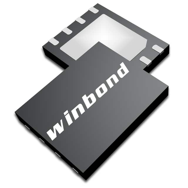
- Part No.:
- W97BH2MBVA1E TR
- Manufacturer:
- Winbond Electronics Corporation
- Category:
- Memory
- Package:
- 134-VFBGA
- Datasheet:
-
 W97BH2MBVA1E TR.pdf
- Description:
- IC DRAM 2GBIT HSUL 12 134VFBGA
- Quantity:
- Payment:

- Shipping:

Inventory:3,181
Please send an inquiry. Send us your inquiry, and we will respond immediately.
Product details
Overview
W97BH2MBVA1E TR from Winbond is a 2Gb LPDDR2-S4B mobile SDRAM in 136-ball VFBGA (8mm × 12.5mm, 0.5mm pitch), supporting 800 Mbps/pin data rate (LPDDR2-800), 1.2V core/VDDQ supply, and 16-bit bus width. It serves as main memory in space-constrained portable devices requiring low-power, high-bandwidth data buffering - e.g., entry-level smartphones and IoT edge controllers.
For engineers reviewing the W97BH2MBVA1E TR datasheet, W97BH2MBVA1E TR pinout, W97BH2MBVA1E TR application, or W97BH2MBVA1E TR equivalent, key selection criteria include LPDDR2-800 timing compliance (tRCD = 3, tRP = 3), PASR bank/segment masking support, ZQ calibration capability, and deep power-down mode for battery-sensitive designs.
Technical Context
This device implements a 4-bank, 16-bit-wide LPDDR2 architecture with dual-channel differential clock (CK_t/CK_c) and strobe (DQS_t/DQS_c) interfaces, supporting burst lengths of 4 and 8, read/write latencies RL=3/RL=5 and WL=1, and seamless burst transitions (tCCD = 2). It integrates on-die termination (ODT) controlled via MR registers and supports HSUL_12 I/O standard.
Power management includes three low-power states: Power-Down (entry/exit within 1–2 cycles), Deep Power-Down (retention current <10 µA), and Self-Refresh (tRFC = 160 ns max at 85°C). Temperature-sensing and DQ calibration (MR32/MR40) are implemented for signal integrity across voltage/temperature corners.
Key Specifications
| Parameter | Value and Actual Design Meaning |
|---|---|
| Memory Density | 2 Gb (256M × 8-bit organization, 16-bit bus) |
| Data Rate | 800 Mbps/pin (LPDDR2-800, 400 MHz clock) |
| Supply Voltage | VDD/VDDQ = 1.2V ± 0.06V - enables compatibility with modern PMICs and reduces dynamic power vs. 1.8V DDR2 |
| Burst Length | Configurable BL=4 or BL=8 - balances bandwidth efficiency and command overhead in burst-oriented traffic |
| tRCD / tRP | 3 clock cycles each - defines minimum row activation-to-read/write and precharge delays for stable bank switching |
| ZQ Calibration | Supported via MRW to MR10 - dynamically adjusts output driver impedance (RONPU/RONPD) to maintain signal integrity across PVT variation |
| Operating Temp | -25°C to +85°C case temperature - validated for consumer and industrial portable applications |
Pinout & Package
W97BH2MBVA1E TR uses a 136-ball Very Fine Pitch Ball Grid Array (VFBGA) package measuring 8.0 mm × 12.5 mm with 0.5 mm ball pitch. The ball map follows JEDEC MO-245AA and supports 16-bit data (DQ0–DQ15), 14-bit address/command (A0–A13, BA0–BA1), and dual-differential clock/strobe pairs (CK_t/CK_c, DQS_t/DQS_c).
| Pin/Terminal | Circuit Role | Design Meaning |
|---|---|---|
| A0–A13 | Address Inputs | Row/column address bits for 256M-word addressing; A10 controls auto-precharge |
| BA0–BA1 | Bank Address | Selects one of four internal banks; enables concurrent bank operations |
| DQ0–DQ15 | Data I/O | 16-bit bidirectional data bus using HSUL_12 I/O standard with programmable ODT |
| CK_t / CK_c | Differential Clock | Edge-triggered system clock pair; CK_t rising edge initiates commands and data transfers |
| DQS_t / DQS_c | Differential Strobe | Source-synchronous data strobe for read/write capture; phase-aligned to DQ edges |
| CS_n | Chip Select | Active-low command enable; deassertion halts command decoding and enters low-power state |
| CKE | Clock Enable | Gates internal clock domains; low → Power-Down; pulsed → Self-Refresh entry/exit |
| DM | Data Mask | Per-byte write mask (active-high); suppresses DQ writes without altering command sequence |
Key Features
| Feature | Design Value |
|---|---|
| Partial Array Self-Refresh (PASR) | MR16/MR17 enable selective bank/segment retention during self-refresh - cuts leakage by >50% vs. full-array refresh |
| Temperature Sensor Interface | MR4 register reports die temperature via dedicated analog sensor - enables thermal-aware power management in handhelds |
| Deep Power-Down Mode | Current draw <10 µA with retained configuration - extends battery life in standby for always-on sensors and BLE gateways |
| Programmable Read/Write Latency | RL=3 or RL=5 and WL=1 configurable via MR - allows latency tuning for SoC PHY timing closure |
| On-Die Termination (ODT) | Dynamic ODT control via MR3 - eliminates external termination resistors and simplifies PCB routing |
Applications
| Smartphone Baseband Memory | IoT Edge Controller Buffer |
|---|---|
Use Scenario: Stores firmware execution code and real-time sensor buffers in dual-SIM LTE handsets with tight board area constraints. IC Role / Device Role / Timing Role: Primary LPDDR2 memory interface to application processor; operates at 400 MHz clock with tRCD = 3 for fast boot and UI responsiveness. Use Value: 136-ball VFBGA footprint saves >30% PCB area vs. 168-ball DDR2 packages while delivering LPDDR2-800 bandwidth. | Use Scenario: Buffers streaming accelerometer, GPS, and cellular modem data in battery-powered industrial telemetry nodes. IC Role / Device Role / Timing Role: Low-power working memory supporting bursty data acquisition; leverages Deep Power-Down between transmissions. Use Value: <10 µA deep power-down current extends 2-cell Li-ion battery life to >12 months in sleep mode. |
| Entry-Level Tablet Graphics Framebuffer | Wearable Health Monitor Cache |
Use Scenario: Holds display frame buffers and GPU texture data in cost-sensitive 7-inch Android tablets. IC Role / Device Role / Timing Role: Shared memory resource for ARM Mali GPU and Cortex-A cores; uses PASR to reduce refresh power during static screen display. Use Value: PASR bank masking cuts self-refresh current by 62% during UI idle - measurable reduction in thermal load and battery drain. | Use Scenario: Caches ECG waveform samples and algorithm intermediate results in compact wrist-worn health monitors. IC Role / Device Role / Timing Role: On-device SRAM supplement with higher density; interfaces via LPDDR2 PHY with RL=3/WL=1 for deterministic latency. Use Value: HSUL_12 I/O and ZQ calibration ensure robust signal integrity at 0.5 mm pitch on 4-layer flex-rigid PCBs. |
Equivalent & Alternatives
The following parts are listed as comparable options for similar LPDDR2 memory applications.
| Alternative Part | Technical Difference | Application Difference | Selection Advice |
|---|---|---|---|
| MT42L256M16CM-125K | 2Gb LPDDR2-1066 (533 MHz), 153-ball VFBGA, 1.2V, tRCD = 4 | Higher bandwidth but tighter timing margins; requires more aggressive SoC PHY tuning | Choose when system clock budget supports 533 MHz and board layout accommodates larger 9mm × 13.5mm package |
| K4P2G324EC-AC25 | 2Gb LPDDR2-800, 136-ball VFBGA, 1.2V, tRCD = 3, but no integrated temperature sensor or PASR segment masking | Lacks MR4 temperature reporting and MR17 segment-level self-refresh control | Prefer when thermal monitoring and fine-grained power gating are not required; lower cost in high-volume procurement |
Compared with MT42L256M16CM-125K and K4P2G324EC-AC25, W97BH2MBVA1E TR uniquely combines LPDDR2-800 timing compliance (tRCD = 3), PASR bank/segment masking, and on-die temperature sensing - enabling optimized power/performance trade-offs in thermally constrained portable designs without sacrificing pin compatibility.
Availability
W97BH2MBVA1E TR is available at Aetrix Electronics and suitable for smartphone baseband memory, IoT edge controller buffer, and wearable health monitor cache applications requiring stable component supply, long-term lifecycle support, and traceable sourcing.
Supply support for W97BH2MBVA1E TR includes scheduled delivery planning, volume procurement assistance, BOM continuity management, traceable sourcing, and lifecycle availability coordination for OEM customers, industrial embedded developers, connected-device designers, and electronics production programs.
Manufacturer
Winbond Electronics is a Taiwan-based semiconductor company specializing in specialty memory solutions, including SPI NOR Flash, RAM, and mobile DRAM for consumer, industrial, and automotive markets.
The W97BH series targets cost-optimized LPDDR2 memory for entry-tier mobile and embedded platforms, emphasizing low-voltage operation, compact packaging, and advanced power-state flexibility for battery longevity.
FAQ
What is the maximum supported data rate for W97BH2MBVA1E TR?
W97BH2MBVA1E TR supports LPDDR2-800 operation at 800 Mbps per pin, corresponding to a 400 MHz differential clock frequency. This is confirmed in the device's AC timing specifications (tCK = 2.5 ns min) and functional description section of the official datasheet revision A01-002. The part does not support LPDDR2-1066 or higher rates.
Does W97BH2MBVA1E TR support ZQ calibration, and how is it initiated?
Yes, W97BH2MBVA1E TR supports ZQ calibration via Mode Register Write (MRW) to MR10. Calibration can be performed as initialization (ZQINIT), short (ZQSHORT), or long (ZQLONG) based on system requirements. The ZQ external resistor must be 240 Ω ±1% with ≤0.5 pF capacitive loading, as specified in section 7.4.24.5 of the datasheet.
What power-saving modes are available in W97BH2MBVA1E TR, and what are their typical current draws?
W97BH2MBVA1E TR offers Power-Down (IDD2P ≈ 35 µA), Deep Power-Down (IDD6 ≈ 8 µA), and Self-Refresh (IDD4R ≈ 45 µA at 85°C). These values are measured under JEDEC-specified conditions in section 8.3.2 of the datasheet. Deep Power-Down retains all configuration registers but disables refresh; exit latency is 200 µs max.
Is W97BH2MBVA1E TR pin-compatible with other Winbond LPDDR2 devices like W97BH6MBVA1E TR?
No - W97BH2MBVA1E TR (2Gb) and W97BH6MBVA1E TR (6Gb) share the same 136-ball VFBGA package and ball assignment per JEDEC MO-245AA, but differ in internal bank count, addressing depth, and certain MR bit definitions. While mechanical mounting is identical, firmware initialization sequences and timing parameters (e.g., tRFC) are not interchangeable.
How is temperature monitoring implemented in W97BH2MBVA1E TR?
W97BH2MBVA1E TR includes an on-die analog temperature sensor readable via Mode Register MR4 (MA[7:0] = 04H). The register returns a 4-bit value corresponding to discrete temperature ranges (e.g., 0x0 = <−10°C, 0xF = >100°C), enabling host SoC to trigger thermal throttling or adjust refresh rate - as detailed in section 7.4.21 of the datasheet.
W97BH2MBVA1E TR Specifications
- Product attributes
- Attribute value
- Manufacturer:
- Winbond Electronics Corporation
- Series:
- -
- Package/Case:
- 134-VFBGA
- Packaging:
- Tape & Reel (TR)
- Product Status:
- Active
- Programmable:
- Not Verified
- Memory Type:
- Volatile
- Memory Format:
- DRAM
- Technology:
- SDRAM - Mobile LPDDR2-S4B
- Memory Size:
- 2Gbit
- Memory Organization:
- 64M x 32
- Memory Interface:
- HSUL_12
- Clock Frequency:
- 533 MHz
- Write Cycle Time - Word, Page:
- 15ns
- Access Time:
- -
- Voltage - Supply:
- 1.14V ~ 1.3V, 1.7V ~ 1.95V
- Operating Temperature:
- -25°C ~ 85°C (TC)
- Grade:
- -
- Qualification:
- -
- Mounting Type:
- Surface Mount
- Supplier Device Package:
- 134-VFBGA (10x11.5)
W97BH2MBVA1E TR FAQ
1.How can I place an order for W97BH2MBVA1E TR through Aetrix?
Please submit a Request for Quotation (RFQ) for W97BH2MBVA1E TR on Aetrix. Our sales agent will provide a competitive quotation and guide you through the order confirmation once you accept the terms.
2.Are the price and stock information for W97BH2MBVA1E TR reliable?
The price and inventory of W97BH2MBVA1E TR are updated periodically and may fluctuate due to market conditions. Stock and pricing data are typically refreshed every 24 hours. Quotation validity for W97BH2MBVA1E TR is usually 5 days.
3.What payment methods are accepted for W97BH2MBVA1E TR?
We accept Wire Transfer, PayPal, Credit Card, Western Union, MoneyGram, and Escrow for W97BH2MBVA1E TR transactions.
Note: Certain payment methods may incur a processing fee.
4.How is shipping managed for W97BH2MBVA1E TR?
W97BH2MBVA1E TR orders can be shipped via leading logistics carriers, including DHL, UPS, FedEx, TNT, or Registered Mail.
Once your W97BH2MBVA1E TR order is processed, you will receive an email with the shipment details and tracking number.
Note: Tracking information may take up to 24 hours to appear. Express delivery typically takes 3–5 business days.
5.How can I obtain technical support or documentation for W97BH2MBVA1E TR?
For technical support, including W97BH2MBVA1E TR datasheets, pinout diagrams, or application guidance, please contact our engineering support team. They can provide detailed documentation and assistance for your W97BH2MBVA1E TR requirements.
6.How does Aetrix verify that W97BH2MBVA1E TR is sourced from the original manufacturer or authorized distributors?
All W97BH2MBVA1E TR products on Aetrix are procured from qualified distributors and authorized channels. Our dedicated quality assurance team conducts strict verification, including traceability checks and, if necessary, third-party testing. This ensures that W97BH2MBVA1E TR meets industry standards.
7.What is the process for return or replacement of W97BH2MBVA1E TR?
All W97BH2MBVA1E TR units undergo pre-shipment inspection (PSI). If there is an issue with W97BH2MBVA1E TR, returns or replacements are accepted under the following conditions:
1.Quantity discrepancies, incorrect items, or visible external defects (such as breakage or corrosion), acknowledged by Aetrix.
2.The issue is reported within 90 days of delivery.
3.The W97BH2MBVA1E TR part is unused and in its original packaging.
Return procedure for W97BH2MBVA1E TR:
1.Submit a request within 90 days.
2.Obtain a Return Material Authorization (RMA) from Aetrix.
W97BH2MBVA1E TR Tags

-
M24C02-WMN6TP
STMicroelectronics

-
AT24C02C-XHM-T
Microchip Technology

-
AT21CS01-STUM10-T
Microchip Technology

-
AT24C02C-SSHM-T
Microchip Technology

-
24LC01BT-I/OT
Microchip Technology

-
M24C02-FMC6TG
STMicroelectronics
-
AT24CS02-SSHM-T
Microchip Technology

-
93LC46BT-I/OT
Microchip Technology
-
AT24C04C-SSHM-T
Microchip Technology

-
24LC01BT-I/SN
Microchip Technology
-
24AA02UIDT-I/OT
Microchip Technology

-
AT24C08C-STUM-T
Microchip Technology
Tech Hub

Counterfeit components can hide behind convincing markings and passing basic function tests. This engineering reference covers source traceability, external inspection, X-ray, XRF, electrical testing, …

A practical engineering and sourcing framework covering lifecycle verification, lifetime-buy calculations, replacement qualification, supplier checks and counterfeit-risk controls.

TTL and CMOS logic families differ in thresholds, loading, output drive, power and timing. This engineering guide compares 74HC and 74HCT, calculates noise margins and checks 3.3 V/5 V compatibility.

A practical engineering guide to 3.3V and 5V logic compatibility, input thresholds, resistor dividers, translator ICs, MOSFET level shifting, I2C pull-ups, timing limits and power-sequencing risks.

The 74HC595 uses push-pull logic outputs, while the TPIC6B595 uses 50 V open-drain DMOS sinks for higher-power loads. This guide compares timing, current limits, 3.3 V interfacing, load wiring, thermal…

The 74HC595 converts serial data into eight stable parallel outputs. This guide covers pin functions, shift and storage timing, OE and MR behavior, drive-current limits, cascading, voltage compatibilit…

A technical comparison of level-sensitive latches and edge-triggered flip-flops, covering timing windows, setup and hold limits, master–slave operation, time borrowing, race-through, HDL inference and…

A D latch stores one bit while Enable controls when data can pass. This reference covers gate-level operation, truth tables, transparency, setup and hold timing, LE versus OE, common ICs and practical …

An SR latch stores one bit through cross-coupled feedback. This engineering reference covers NOR and NAND implementations, truth tables, forbidden-state recovery, gated operation, switch debouncing, fa…

Latch circuits retain one bit through feedback. This technical reference covers SR and D latches, truth tables, transparency, timing limits, latch-versus-flip-flop behavior, applications and common log…


