
 My Inquiry
 My Account


Winbond Electronics Corporation W9816G6JH-6 TR
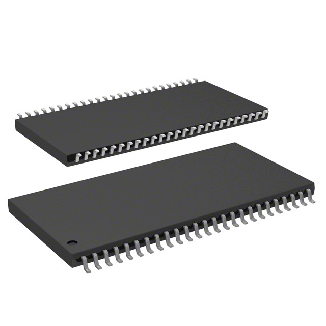
- Part No.:
- W9816G6JH-6 TR
- Manufacturer:
- Winbond Electronics Corporation
- Category:
- Memory
- Package:
- 50-TSOP (0.400", 10.16mm Width)
- Datasheet:
-
 W9816G6JH-6 TR.pdf
- Description:
- IC DRAM 16MBIT PAR 50TSOP II
- Quantity:
- Payment:

- Shipping:

Inventory:4,035
Please send an inquiry. Send us your inquiry, and we will respond immediately.
Product details
Overview
W9816G6JH-6 TR from Winbond is a 512K × 2 banks × 16-bit synchronous DRAM (SDRAM) operating at 166 MHz with CAS Latency 3, 3.3V ±0.3V supply, and LVTTL interface. It delivers 332 MB/s peak bandwidth in burst-4 mode and supports auto-precharge, self-refresh, and interleaved bank access for high-efficiency memory subsystems in embedded controllers and industrial displays.
For engineers reviewing the W9816G6JH-6 TR datasheet, W9816G6JH-6 TR pinout, W9816G6JH-6 TR application, or W9816G6JH-6 TR equivalent, key selection criteria include its TSOP II-50 package, -6 speed grade timing compliance (tRCD = 20 ns, tRP = 20 ns), burst length configurability (1/2/4/8/full page), and dual DQM masking for byte-level write control in resource-constrained systems.
Technical Context
This SDRAM implements a two-bank architecture with independent row activation and column access, enabling true bank interleaving to hide precharge latency. Its programmable Mode Register controls burst type (sequential/interleaved), burst length, and CAS latency-critical for optimizing throughput in burst-oriented data paths like video frame buffers or network packet queues.
Command decoding is fully synchronous to CLK, with all operations triggered on rising edges. The device supports power management via CKE-controlled Power Down and Self Refresh modes, and uses separate VDDQ/VSSQ rails to isolate I/O noise from core logic-essential for stable operation in mixed-signal industrial environments.
Key Specifications
| Parameter | Value and Actual Design Meaning |
|---|---|
| Memory Organization | 524,288 words × 2 banks × 16 bits = 16 Mbit total capacity; enables 16-bit wide data transfers without external multiplexing. |
| Max Clock Frequency | 166 MHz (–6 grade); defines maximum system bus clock rate and sets tCK = 6 ns timing constraint for all AC parameters. |
| CAS Latency | CL = 3 cycles; determines minimum read-to-data-valid delay (tAC = 5.4 ns typical), critical for CPU/cache coherency timing. |
| Burst Length | Programmable 1/2/4/8/full page; allows optimization between latency (short bursts) and bandwidth efficiency (long bursts). |
| Refresh Requirement | 2,048 cycles / 32 ms (64 ms refresh interval); mandates periodic refresh command issuance to retain data integrity. |
| I/O Interface | LVTTL-compatible; ensures direct interfacing with 3.3V microcontrollers and FPGAs without level-shifting circuitry. |
| Supply Voltage | 3.0 V to 3.6 V (VDD/VDDQ); supports standard 3.3V rail with ±10% tolerance, simplifying power design. |
| Operating Temperature | 0°C to +70°C; validated for commercial-grade applications including industrial HMIs and communication gateways. |
Pinout & Package
W9816G6JH-6 TR is housed in a 50-pin, 400-mil TSOP II package with lead-free, RoHS-compliant construction. Pin layout follows JEDEC-standard SDRAM pinout for mechanical and thermal compatibility with legacy PCB footprints.
| Pin/Terminal | Circuit Role | Design Meaning |
|---|---|---|
| A0–A10 | Address Input (multiplexed) | Row/column address lines shared across banks; A0–A10 used for row, A0–A7 for column addressing. |
| BA | Bank Address | Selects one of two internal banks during ACTIVATE or READ/WRITE commands; enables bank interleaving. |
| DQ0–DQ15 | Data I/O | 16-bit bidirectional data bus; supports simultaneous read/write with LDQM/UDQM for byte masking. |
| CS, RAS, CAS, WE | Command Control | Four active-low control signals defining all operations (e.g., CS+RAS+CAS+WE = MODE REGISTER SET). |
| CLK, CKE | Clock Interface | CLK synchronizes all inputs; CKE gates clock domain entry/exit for Power Down and Self Refresh modes. |
| LDQM / UDQM | Data Mask | Low/high byte mask inputs; tri-state outputs or block writes with zero latency during write cycles. |
| VDD / VSS | Core Power / Ground | Supplies logic circuitry; requires local decoupling near pins 1/25 and 26/50 per layout guidelines. |
| VDDQ / VSSQ | I/O Power / Ground | Separate analog-like supply for DQ drivers; reduces switching noise coupling into core logic. |
Key Features
| Feature | Design Value |
|---|---|
| Interleaved Bank Access | Enables continuous data streaming across banks by overlapping precharge and activate phases-reducing effective access latency by up to 40% vs single-bank operation. |
| Programmable Burst Mode | Supports sequential or interleaved burst addressing; allows matching memory access pattern to processor cache line size (e.g., burst-4 for 64-byte lines). |
| Auto-Precharge | Automatically initiates bank precharge after burst completion when A10 = HIGH; eliminates need for explicit PRECHARGE command in pipelined read/write sequences. |
| Dual DQM Control | Independent LDQM (lower byte) and UDQM (upper byte) enable selective 8-bit masking-critical for mixed-endian or partial-word update scenarios. |
| Self-Refresh Mode | Retains data with <2 mA current draw while suspending external clocks; supports low-power standby in battery-backed industrial controllers. |
| TSOP II Mechanical Compatibility | 50-pin 400-mil footprint matches industry-standard SDRAM layouts-enabling drop-in replacement in existing designs using compatible density parts. |
Applications
| Industrial HMI Display Buffer | Network Packet Buffer |
|---|---|
|
Use Scenario: Storing frame buffers for 800×480 TFT panels in factory-floor HMIs with real-time UI updates. IC Role / Device Role / Timing Role: Primary graphics memory providing 16-bit parallel pixel data at 60 Hz refresh; synchronized to display controller's pixel clock via CLK/CKE handshake. Use Value: Interleaved bank access sustains >280 MB/s sustained read bandwidth-exceeding required 230 MB/s for full-screen updates without frame tearing. |
Use Scenario: Temporary storage of Ethernet frames in industrial gateways before routing or protocol translation. IC Role / Device Role / Timing Role: Dual-port buffer supporting concurrent ingress (MAC-side write) and egress (CPU-side read) via bank separation. Use Value: Auto-precharge and burst-8 mode reduce average packet write latency to ≤1.2 µs-enabling line-rate 100 Mbps forwarding with minimal jitter. |
| Embedded Media Decoder | PLC Logic Execution Memory |
|
Use Scenario: Holding decoded MPEG-2 video streams in set-top boxes or digital signage players. IC Role / Device Role / Timing Role: High-bandwidth streaming buffer feeding video DSP cores; configured for sequential burst reads aligned to macroblock boundaries. Use Value: CAS Latency 3 and tRCD = 20 ns ensure deterministic 166 MHz read response-meeting tight 125 ns deadline for 4:2:0 chroma subsampling pipelines. |
Use Scenario: Storing ladder logic state tables and I/O image registers in modular PLCs with deterministic scan cycles. IC Role / Device Role / Timing Role: Non-volatile shadow RAM accessed via microcontroller's external bus interface; refreshed autonomously during idle scan periods. Use Value: Self-refresh current ≤2 mA extends backup battery life to >72 hours during AC power loss-meeting IEC 61131-2 uptime requirements. |
Equivalent & Alternatives
The following parts are listed as comparable options for similar SDRAM applications.
| Alternative Part | Technical Difference | Application Difference | Selection Advice |
|---|---|---|---|
| IS42S16100E-6BLI | Same 16Mbit organization, 54-pin TSOP, but rated for -40°C to +85°C industrial temp range; tRC = 60 ns vs 66 ns. | Better suited for extended temperature deployments (e.g., outdoor kiosks); requires PCB pad revision due to 54-pin count. | Choose for wider temperature operation where board redesign is acceptable. |
| MT48LC16M16A2P-6A:G | Identical 512K×2×16 structure and -6 speed grade, but 54-pin TSOP; higher IDD2 (110 mA vs 95 mA typical) and no LDQM/UDQM separation. | Compatible timing but lacks independent byte masking-requires software workarounds for partial writes. | Choose only if existing design already uses Micron's pinout and masking constraints are not critical. |
Compared with IS42S16100E-6BLI and MT48LC16M16A2P-6A:G, W9816G6JH-6 TR offers native 50-pin TSOP II compatibility and dual DQM control-reducing PCB layer count and simplifying partial-write logic in cost-sensitive industrial controllers.
Availability
W9816G6JH-6 TR is available at Aetrix Electronics and suitable for industrial HMIs, network gateways, embedded media players, and PLC controllers requiring stable component supply across multi-year production cycles.
Supply support for W9816G6JH-6 TR includes scheduled delivery planning, volume procurement assistance, BOM continuity management, traceable sourcing, and lifecycle availability coordination for OEM customers, industrial embedded developers, connected-device designers, and electronics production programs.
Manufacturer
Winbond Electronics is a Taiwan-based semiconductor manufacturer specializing in memory ICs, flash storage, and security solutions, with over 30 years of DRAM design heritage.
The W9816G6JH series targets cost-optimized, high-reliability embedded systems requiring standardized SDRAM performance without premium pricing-emphasizing industrial temperature variants and long-lifecycle support.
FAQ
What is the maximum operating frequency supported by W9816G6JH-6 TR?
W9816G6JH-6 TR supports a maximum clock frequency of 166 MHz, corresponding to a 6 ns clock period (tCK). This speed grade meets PC133 SDRAM timing specifications and is validated for stable operation under 3.3V ±0.3V supply with CAS Latency 3. All AC timing parameters-including tRCD, tRP, and tRC-are guaranteed at this frequency across the 0°C to +70°C operating range.
Does W9816G6JH-6 TR support both sequential and interleaved burst addressing modes?
Yes, W9816G6JH-6 TR supports both sequential and interleaved burst addressing, controlled via the Mode Register. Sequential mode increments column addresses linearly (e.g., n, n+1, n+2), while interleaved mode toggles lower address bits for cache-friendly access patterns. This flexibility allows optimization for different processor architectures-such as ARM Cortex-A series (preferring sequential) or legacy x86 derivatives (benefiting from interleaved).
How does the auto-precharge function operate in W9816G6JH-6 TR?
In W9816G6JH-6 TR, auto-precharge is activated by setting A10 = HIGH during a READ or WRITE command. For reads, precharge begins before burst completion (delayed by CAS Latency cycles); for writes, it starts two clocks after final data input (tWR). This eliminates manual PRECHARGE command insertion, reducing command overhead in burst-intensive applications like video streaming or DMA transfers.
What is the purpose of separate VDDQ and VSSQ pins on W9816G6JH-6 TR?
W9816G6JH-6 TR uses dedicated VDDQ and VSSQ pins to isolate I/O buffer power from core logic supplies. This separation minimizes noise coupling from high-speed DQ switching into sensitive internal circuits, improving signal integrity and timing margin-especially critical in mixed-signal industrial environments where EMI immunity directly impacts system reliability.
Can W9816G6JH-6 TR be used in systems requiring extended temperature operation?
No, W9816G6JH-6 TR is specified for 0°C to +70°C operation only. For extended temperature applications (–40°C to +85°C), the pin-compatible W9816G6JH-6I variant must be selected. The -6I version shares identical electrical and timing characteristics but undergoes additional screening and qualification to guarantee performance across the industrial temperature range.
W9816G6JH-6 TR Specifications
- Product attributes
- Attribute value
- Manufacturer:
- Winbond Electronics Corporation
- Series:
- -
- Package/Case:
- 50-TSOP (0.400", 10.16mm Width)
- Packaging:
- Tape & Reel (TR)
- Product Status:
- Not For New Designs
- Programmable:
- Not Verified
- Memory Type:
- Volatile
- Memory Format:
- DRAM
- Technology:
- SDRAM
- Memory Size:
- 16Mbit
- Memory Organization:
- 1M x 16
- Memory Interface:
- Parallel
- Clock Frequency:
- 166 MHz
- Write Cycle Time - Word, Page:
- -
- Access Time:
- 5 ns
- Voltage - Supply:
- 3V ~ 3.6V
- Operating Temperature:
- 0°C ~ 70°C (TA)
- Grade:
- -
- Qualification:
- -
- Mounting Type:
- Surface Mount
- Supplier Device Package:
- 50-TSOP II
W9816G6JH-6 TR FAQ
1.How can I place an order for W9816G6JH-6 TR through Aetrix?
Please submit a Request for Quotation (RFQ) for W9816G6JH-6 TR on Aetrix. Our sales agent will provide a competitive quotation and guide you through the order confirmation once you accept the terms.
2.Are the price and stock information for W9816G6JH-6 TR reliable?
The price and inventory of W9816G6JH-6 TR are updated periodically and may fluctuate due to market conditions. Stock and pricing data are typically refreshed every 24 hours. Quotation validity for W9816G6JH-6 TR is usually 5 days.
3.What payment methods are accepted for W9816G6JH-6 TR?
We accept Wire Transfer, PayPal, Credit Card, Western Union, MoneyGram, and Escrow for W9816G6JH-6 TR transactions.
Note: Certain payment methods may incur a processing fee.
4.How is shipping managed for W9816G6JH-6 TR?
W9816G6JH-6 TR orders can be shipped via leading logistics carriers, including DHL, UPS, FedEx, TNT, or Registered Mail.
Once your W9816G6JH-6 TR order is processed, you will receive an email with the shipment details and tracking number.
Note: Tracking information may take up to 24 hours to appear. Express delivery typically takes 3–5 business days.
5.How can I obtain technical support or documentation for W9816G6JH-6 TR?
For technical support, including W9816G6JH-6 TR datasheets, pinout diagrams, or application guidance, please contact our engineering support team. They can provide detailed documentation and assistance for your W9816G6JH-6 TR requirements.
6.How does Aetrix verify that W9816G6JH-6 TR is sourced from the original manufacturer or authorized distributors?
All W9816G6JH-6 TR products on Aetrix are procured from qualified distributors and authorized channels. Our dedicated quality assurance team conducts strict verification, including traceability checks and, if necessary, third-party testing. This ensures that W9816G6JH-6 TR meets industry standards.
7.What is the process for return or replacement of W9816G6JH-6 TR?
All W9816G6JH-6 TR units undergo pre-shipment inspection (PSI). If there is an issue with W9816G6JH-6 TR, returns or replacements are accepted under the following conditions:
1.Quantity discrepancies, incorrect items, or visible external defects (such as breakage or corrosion), acknowledged by Aetrix.
2.The issue is reported within 90 days of delivery.
3.The W9816G6JH-6 TR part is unused and in its original packaging.
Return procedure for W9816G6JH-6 TR:
1.Submit a request within 90 days.
2.Obtain a Return Material Authorization (RMA) from Aetrix.
W9816G6JH-6 TR Tags

-
M24C02-WMN6TP
STMicroelectronics

-
AT24C02C-XHM-T
Microchip Technology

-
AT21CS01-STUM10-T
Microchip Technology

-
AT24C02C-SSHM-T
Microchip Technology

-
24LC01BT-I/OT
Microchip Technology

-
M24C02-FMC6TG
STMicroelectronics
-
AT24CS02-SSHM-T
Microchip Technology

-
93LC46BT-I/OT
Microchip Technology
-
AT24C04C-SSHM-T
Microchip Technology

-
24LC01BT-I/SN
Microchip Technology
-
24AA02UIDT-I/OT
Microchip Technology

-
AT24C08C-STUM-T
Microchip Technology
Tech Hub

Counterfeit components can hide behind convincing markings and passing basic function tests. This engineering reference covers source traceability, external inspection, X-ray, XRF, electrical testing, …

A practical engineering and sourcing framework covering lifecycle verification, lifetime-buy calculations, replacement qualification, supplier checks and counterfeit-risk controls.

TTL and CMOS logic families differ in thresholds, loading, output drive, power and timing. This engineering guide compares 74HC and 74HCT, calculates noise margins and checks 3.3 V/5 V compatibility.

A practical engineering guide to 3.3V and 5V logic compatibility, input thresholds, resistor dividers, translator ICs, MOSFET level shifting, I2C pull-ups, timing limits and power-sequencing risks.

The 74HC595 uses push-pull logic outputs, while the TPIC6B595 uses 50 V open-drain DMOS sinks for higher-power loads. This guide compares timing, current limits, 3.3 V interfacing, load wiring, thermal…

The 74HC595 converts serial data into eight stable parallel outputs. This guide covers pin functions, shift and storage timing, OE and MR behavior, drive-current limits, cascading, voltage compatibilit…

A technical comparison of level-sensitive latches and edge-triggered flip-flops, covering timing windows, setup and hold limits, master–slave operation, time borrowing, race-through, HDL inference and…

A D latch stores one bit while Enable controls when data can pass. This reference covers gate-level operation, truth tables, transparency, setup and hold timing, LE versus OE, common ICs and practical …

An SR latch stores one bit through cross-coupled feedback. This engineering reference covers NOR and NAND implementations, truth tables, forbidden-state recovery, gated operation, switch debouncing, fa…

Latch circuits retain one bit through feedback. This technical reference covers SR and D latches, truth tables, transparency, timing limits, latch-versus-flip-flop behavior, applications and common log…


