
 My Inquiry
 My Account


Winbond Electronics Corporation W9864G6JT-6I
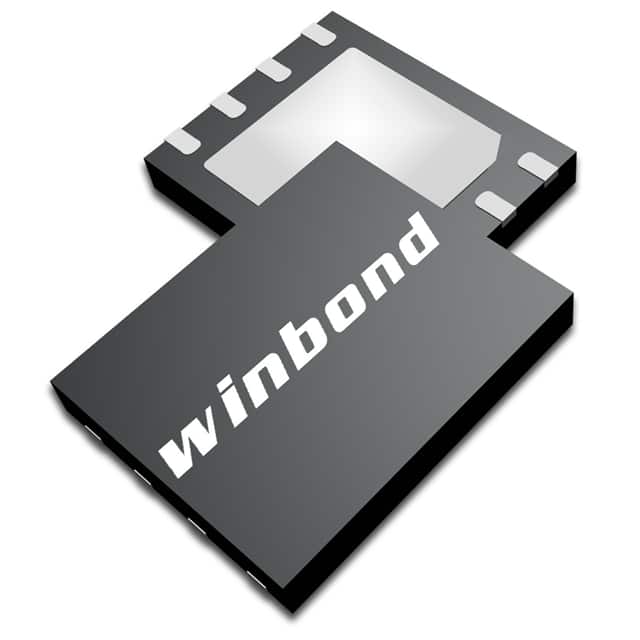
- Part No.:
- W9864G6JT-6I
- Manufacturer:
- Winbond Electronics Corporation
- Category:
- Memory
- Package:
- 54-TFBGA
- Datasheet:
-
 W9864G6JT-6I.pdf
- Description:
- IC DRAM 64MBIT LVTTL 54TFBGA
- Quantity:
- Payment:

- Shipping:

Inventory:3,101
Please send an inquiry. Send us your inquiry, and we will respond immediately.
Product details
Overview
W9864G6JT-6I from Winbond is a 1M × 4 banks × 16-bit synchronous DRAM (SDRAM) operating at 166 MHz with CAS Latency 3, 3.3V LVTTL interface, and industrial temperature range (–40°C to +85°C). It delivers up to 166 million words/second bandwidth and supports burst lengths of 1, 2, 4, 8, or full page for high-throughput memory buffering in embedded controllers and industrial HMIs.
For engineers reviewing the W9864G6JT-6I datasheet, W9864G6JT-6I pinout, W9864G6JT-6I application, or W9864G6JT-6I equivalent, key selection criteria include its TFBGA-54 package, self-refresh capability, programmable mode register, auto-precharge support, and industrial-grade thermal reliability.
Technical Context
The W9864G6JT-6I implements a four-bank architecture with independent row activation and interleaved bank access to hide precharge latency. Its command decoder interprets RAS/CAS/WE/CS combinations on CLK rising edges to execute bank activate, read/write, precharge, auto-refresh, self-refresh, and power-down operations.
It uses multiplexed address pins A0–A11 (row/column), BS0/BS1 for bank selection, and LDQM/UDQM for byte-level write masking. The mode register configures burst type (sequential/interleave), length, and CAS latency - all required to be set post-power-up before normal operation.
Key Specifications
| Parameter | Value and Actual Design Meaning |
|---|---|
| Memory Organization | 1,048,576 words × 4 banks × 16 bits = 128 Mbit total capacity |
| Clock Frequency | 166 MHz - defines maximum data transfer rate and system timing budget |
| CAS Latency | CL = 3 - fixed 3-cycle delay between column address strobe and first valid data output |
| Burst Length | 1, 2, 4, 8, or full page - determines consecutive data words per read/write command |
| Operating Temperature | –40°C to +85°C - validated for industrial environments without derating |
| Supply Voltage | VDD = VDDQ = 3.3V ± 0.3V - requires dual-rail 3.3V supply with separate I/O power (VDDQ/VSSQ) |
| Refresh Requirement | 4,096 cycles / 64 ms - mandates periodic refresh to retain data; self-refresh mode maintains retention with CKE low |
Pinout & Package
W9864G6JT-6I is packaged in an 8 mm × 8 mm TFBGA-54 (lead-free, RoHS-compliant) with 0.8 mm ball pitch.
| Pin/Terminal | Circuit Role | Design Meaning |
|---|---|---|
| A0–A11 | Address Input | Multiplexed row/column address lines; A10 controls all-bank precharge when high during command |
| BS0, BS1 | Bank Select | Selects one of four internal banks during ACTIVATE or READ/WRITE commands |
| DQ0–DQ15 | Data I/O | 16-bit bidirectional data bus; supports byte masking via LDQM/UDQM |
| /CS, /RAS, /CAS, /WE | Command Control | Active-low control signals decoded on CLK rising edge to define operation (e.g., /RAS+/CAS = READ) |
| CLK, CKE | Clock Interface | CLK synchronizes all inputs; CKE enables/disables clock domain - low enters power-down or self-refresh |
| LDQM, UDQM | Data Mask | High during read disables DQ output drivers (Hi-Z); high during write blocks corresponding byte writes |
| VDD, VDDQ, VSS, VSSQ | Power/Ground | VDD/VSS for core logic; VDDQ/VSSQ isolated for I/O buffers to reduce switching noise coupling |
Key Features
| Feature | Design Value |
|---|---|
| Self-Refresh Mode | Retains data with only CKE held low - eliminates external refresh controller overhead in low-power standby |
| Programmable Mode Register | Configures burst type (sequential/interleave), length, and CAS latency - enables optimization for specific access patterns |
| Auto-Precharge | Automatically initiates bank precharge after read/write completion when A10 = high - reduces software overhead and improves throughput |
| Interleaved Bank Access | Enables continuous data streaming across banks by overlapping activate/precharge/read cycles - hides tRC latency |
| LVTTL-Compatible Interface | 3.3V signaling with VIH ≥ 2.0V and VIL ≤ 0.8V - ensures interoperability with standard microcontroller and FPGA I/O banks |
Applications
| Industrial HMI Display Buffer | Embedded Controller Main Memory |
|---|---|
Use Scenario: Storing frame buffers and GUI assets for 7-inch TFT displays in factory-floor HMIs operating continuously at 60 Hz. IC Role / Device Role / Timing Role: Primary SDRAM acting as display memory with burst reads aligned to pixel clock timing and auto-precharge minimizing inter-frame gaps. Use Value: 166 MHz bandwidth sustains 1024×600@60 Hz RGB565 transfers; industrial temp rating ensures reliability in uncooled enclosures. | Use Scenario: Serving as main working memory for ARM9-based PLC controllers running real-time ladder logic and communication stacks. IC Role / Device Role / Timing Role: System RAM interfaced directly to processor AXI bus; configured for CL3/BL4 to balance latency and throughput for mixed code/data access. Use Value: Four-bank interleaving hides tRP/tRC delays during context switches; self-refresh extends battery-backed runtime during brownouts. |
| Network Edge Gateway Cache | Medical Diagnostic Data Buffer |
Use Scenario: Temporary packet buffering in IEEE 802.3af PoE-powered industrial gateways aggregating Modbus TCP and CANopen traffic. IC Role / Device Role / Timing Role: High-speed packet FIFO with burst writes from MAC and sequential reads to CPU; LDQM/UDQM used for partial packet updates. Use Value: Full-page burst mode enables rapid bulk packet loading; TFBGA-54 footprint fits constrained PCB space near Ethernet PHY. | Use Scenario: Capturing raw ultrasound echo data streams (12-bit @ 40 MSPS) in portable diagnostic devices before compression and storage. IC Role / Device Role / Timing Role: Streaming buffer accepting continuous DMA writes with minimal CPU intervention; configured for interleave-mode BL8 reads to feed DSP pipeline. Use Value: 16-bit bus width matches ADC parallel output; –40°C to +85°C rating supports operation in field-deployed battery-powered units. |
Equivalent & Alternatives
The following parts are listed as comparable options for similar SDRAM applications.
| Alternative Part | Technical Difference | Application Difference | Selection Advice |
|---|---|---|---|
| IS42S16160J-6BLI | Same 128 Mbit organization, 166 MHz, CL3, TFBGA-54, but rated –40°C to +85°C with 2.5V core (VDD = 2.5V, VDDQ = 2.5V) | Requires dual 2.5V supplies instead of single 3.3V; lower active current but incompatible voltage rail | Choose if system already uses 2.5V memory rail and needs identical timing/footprint |
| MT48LC16M16A2P-6A:G | 128 Mbit, 166 MHz, CL3, TSOP-54 package (not pin-compatible); VDD = VDDQ = 3.3V | TSOP-54 footprint requires PCB redesign; same electrical interface but different mechanical integration | Choose for through-hole or legacy board upgrades where TFBGA assembly is unavailable |
Compared with IS42S16160J-6BLI and MT48LC16M16A2P-6A:G, the W9864G6JT-6I offers native 3.3V-only operation in a compact TFBGA package, eliminating level-shifting complexity while maintaining industrial temperature compliance - ideal for new designs prioritizing board area and supply simplicity.
Availability
W9864G6JT-6I is available at Aetrix Electronics and suitable for industrial HMIs, embedded controllers, network gateways, and medical data acquisition systems requiring stable component supply across extended temperature ranges and multi-year production cycles.
Supply support for W9864G6JT-6I includes scheduled delivery planning, volume procurement assistance, BOM continuity management, traceable sourcing, and lifecycle availability coordination for OEM customers, industrial embedded developers, connected-device designers, and electronics production programs.
Manufacturer
Winbond Electronics is a Taiwan-based semiconductor company specializing in specialty memory, flash, and logic ICs for industrial, automotive, and computing markets.
The W9864G6JT-6I belongs to Winbond's legacy SDR SDRAM product line, designed specifically for cost-sensitive, thermally demanding embedded systems needing reliable, drop-in DDR1-era memory performance without advanced features like DLL or differential clocks.
FAQ
What is the minimum setup time for address and control signals relative to CLK for W9864G6JT-6I?
The W9864G6JT-6I requires address (A0–A11, BS0/BS1) and control (/CS, /RAS, /CAS, /WE) signals to be stable for at least 2.5 ns before the CLK rising edge under 166 MHz operation. This setup time is specified in the AC Characteristics table (tIS) and must be met to ensure reliable command registration - failure risks command misinterpretation or initialization failure. The W9864G6JT-6I does not include internal delay-locked loop (DLL) compensation, so PCB trace matching and careful timing closure are essential.
Does W9864G6JT-6I support both sequential and interleaved burst modes, and how is the mode selected?
Yes, W9864G6JT-6I supports both sequential and interleaved burst addressing, selected exclusively via bit M3 in the mode register during the Mode Register Set command. Sequential mode increments column addresses linearly (e.g., n, n+1, n+2); interleaved mode toggles LSBs in a defined pattern. The W9864G6JT-6I does not auto-detect burst type - the host controller must program M3 correctly before any burst access, and the setting persists until reprogrammed.
Can W9864G6JT-6I operate without external refresh circuitry, and what is the self-refresh current draw?
Yes, W9864G6JT-6I supports self-refresh mode: assert /CS, /RAS, /CAS, and CKE low while holding /WE high on a CLK rising edge, then maintain CKE low. In this state, it autonomously manages refresh with no external commands. The datasheet specifies max 2 mA current during self-refresh at TA = 85°C - significantly lower than active-mode current, enabling extended low-power hold states. The W9864G6JT-6I retains full data integrity throughout self-refresh as long as CKE remains low and VDD/VDDQ are maintained.
What is the function of A10 during a READ command, and how does it affect W9864G6JT-6I behavior?
On W9864G6JT-6I, A10 determines auto-precharge activation during READ and WRITE commands. When A10 = high at command registration, the selected bank automatically begins precharging after burst completion - eliminating need for explicit PRECHARGE command. If A10 = low, the bank remains active for subsequent accesses. This behavior is hardwired in W9864G6JT-6I's command decoder and applies identically across all speed grades and temperature ranges.
Is W9864G6JT-6I pin-compatible with other Winbond SDRAMs such as W9825G6JH-6?
No, W9864G6JT-6I is not pin-compatible with W9825G6JH-6. Although both are Winbond SDR SDRAMs in TFBGA-54 packages, W9825G6JH-6 is a 32 Mbit (2M × 4 × 4) device with different address pin count (A0–A12 vs. A0–A11) and distinct ball mapping - confirmed by comparing their respective ball configuration diagrams. Interchanging them would cause address decoding errors and functional failure. The W9864G6JT-6I must be used only with its validated layout and signal routing.
W9864G6JT-6I Specifications
- Product attributes
- Attribute value
- Manufacturer:
- Winbond Electronics Corporation
- Series:
- -
- Package/Case:
- 54-TFBGA
- Packaging:
- Tray
- Product Status:
- Not For New Designs
- Programmable:
- Not Verified
- Memory Type:
- Volatile
- Memory Format:
- DRAM
- Technology:
- SDRAM
- Memory Size:
- 64Mbit
- Memory Organization:
- 4M x 16
- Memory Interface:
- LVTTL
- Clock Frequency:
- 166 MHz
- Write Cycle Time - Word, Page:
- -
- Access Time:
- 5 ns
- Voltage - Supply:
- 3V ~ 3.6V
- Operating Temperature:
- -40°C ~ 85°C (TA)
- Grade:
- -
- Qualification:
- -
- Mounting Type:
- Surface Mount
- Supplier Device Package:
- 54-TFBGA (8x8)
W9864G6JT-6I FAQ
1.How can I place an order for W9864G6JT-6I through Aetrix?
Please submit a Request for Quotation (RFQ) for W9864G6JT-6I on Aetrix. Our sales agent will provide a competitive quotation and guide you through the order confirmation once you accept the terms.
2.Are the price and stock information for W9864G6JT-6I reliable?
The price and inventory of W9864G6JT-6I are updated periodically and may fluctuate due to market conditions. Stock and pricing data are typically refreshed every 24 hours. Quotation validity for W9864G6JT-6I is usually 5 days.
3.What payment methods are accepted for W9864G6JT-6I?
We accept Wire Transfer, PayPal, Credit Card, Western Union, MoneyGram, and Escrow for W9864G6JT-6I transactions.
Note: Certain payment methods may incur a processing fee.
4.How is shipping managed for W9864G6JT-6I?
W9864G6JT-6I orders can be shipped via leading logistics carriers, including DHL, UPS, FedEx, TNT, or Registered Mail.
Once your W9864G6JT-6I order is processed, you will receive an email with the shipment details and tracking number.
Note: Tracking information may take up to 24 hours to appear. Express delivery typically takes 3–5 business days.
5.How can I obtain technical support or documentation for W9864G6JT-6I?
For technical support, including W9864G6JT-6I datasheets, pinout diagrams, or application guidance, please contact our engineering support team. They can provide detailed documentation and assistance for your W9864G6JT-6I requirements.
6.How does Aetrix verify that W9864G6JT-6I is sourced from the original manufacturer or authorized distributors?
All W9864G6JT-6I products on Aetrix are procured from qualified distributors and authorized channels. Our dedicated quality assurance team conducts strict verification, including traceability checks and, if necessary, third-party testing. This ensures that W9864G6JT-6I meets industry standards.
7.What is the process for return or replacement of W9864G6JT-6I?
All W9864G6JT-6I units undergo pre-shipment inspection (PSI). If there is an issue with W9864G6JT-6I, returns or replacements are accepted under the following conditions:
1.Quantity discrepancies, incorrect items, or visible external defects (such as breakage or corrosion), acknowledged by Aetrix.
2.The issue is reported within 90 days of delivery.
3.The W9864G6JT-6I part is unused and in its original packaging.
Return procedure for W9864G6JT-6I:
1.Submit a request within 90 days.
2.Obtain a Return Material Authorization (RMA) from Aetrix.
W9864G6JT-6I Tags

-
M24C02-WMN6TP
STMicroelectronics

-
AT24C02C-XHM-T
Microchip Technology

-
AT21CS01-STUM10-T
Microchip Technology

-
AT24C02C-SSHM-T
Microchip Technology

-
24LC01BT-I/OT
Microchip Technology

-
M24C02-FMC6TG
STMicroelectronics
-
AT24CS02-SSHM-T
Microchip Technology

-
93LC46BT-I/OT
Microchip Technology
-
AT24C04C-SSHM-T
Microchip Technology

-
24LC01BT-I/SN
Microchip Technology
-
24AA02UIDT-I/OT
Microchip Technology

-
AT24C08C-STUM-T
Microchip Technology
Tech Hub

Counterfeit components can hide behind convincing markings and passing basic function tests. This engineering reference covers source traceability, external inspection, X-ray, XRF, electrical testing, …

A practical engineering and sourcing framework covering lifecycle verification, lifetime-buy calculations, replacement qualification, supplier checks and counterfeit-risk controls.

TTL and CMOS logic families differ in thresholds, loading, output drive, power and timing. This engineering guide compares 74HC and 74HCT, calculates noise margins and checks 3.3 V/5 V compatibility.

A practical engineering guide to 3.3V and 5V logic compatibility, input thresholds, resistor dividers, translator ICs, MOSFET level shifting, I2C pull-ups, timing limits and power-sequencing risks.

The 74HC595 uses push-pull logic outputs, while the TPIC6B595 uses 50 V open-drain DMOS sinks for higher-power loads. This guide compares timing, current limits, 3.3 V interfacing, load wiring, thermal…

The 74HC595 converts serial data into eight stable parallel outputs. This guide covers pin functions, shift and storage timing, OE and MR behavior, drive-current limits, cascading, voltage compatibilit…

A technical comparison of level-sensitive latches and edge-triggered flip-flops, covering timing windows, setup and hold limits, master–slave operation, time borrowing, race-through, HDL inference and…

A D latch stores one bit while Enable controls when data can pass. This reference covers gate-level operation, truth tables, transparency, setup and hold timing, LE versus OE, common ICs and practical …

An SR latch stores one bit through cross-coupled feedback. This engineering reference covers NOR and NAND implementations, truth tables, forbidden-state recovery, gated operation, switch debouncing, fa…

Latch circuits retain one bit through feedback. This technical reference covers SR and D latches, truth tables, transparency, timing limits, latch-versus-flip-flop behavior, applications and common log…


