
 My Inquiry
 My Account


Winbond Electronics Corporation W989D6DBGX6I
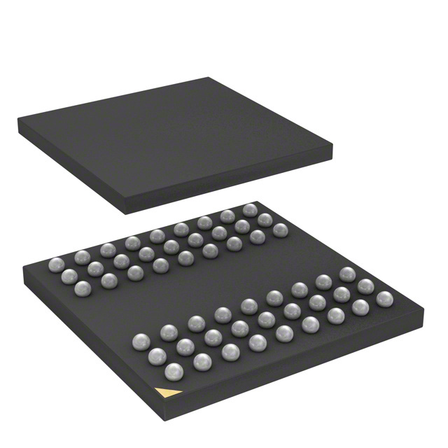
- Part No.:
- W989D6DBGX6I
- Manufacturer:
- Winbond Electronics Corporation
- Category:
- Memory
- Package:
- 54-TFBGA
- Datasheet:
-
 W989D6DBGX6I.pdf
- Description:
- IC DRAM 512MBIT PAR 54VFBGA
- Quantity:
- Payment:

- Shipping:

Inventory:4,463
Please send an inquiry. Send us your inquiry, and we will respond immediately.
Product details
Overview
W989D6DBGX6I from Winbond is a 512Mb (4M × 4 banks × 16-bit) low-power synchronous DRAM IC designed for battery-powered mobile applications. It operates at 1.8V, supports 166MHz clock frequency (−6 speed grade), delivers CAS latency of 2 or 3, and implements Partial Array Self Refresh (PASR) and Automatic Temperature Compensated Self Refresh (ATCSR) to minimize active and standby power in handheld devices like smartphones and digital cameras.
For engineers reviewing the W989D6DBGX6I datasheet, W989D6DBGX6I pinout, W989D6DBGX6I application, or W989D6DBGX6I equivalent, key selection criteria include its 54-ball VFBGA x16 package, industrial temperature range (−40°C to +85°C), LVCMOS-compatible interface, burst length programmability (1/2/4/8/full page), and deep power-down mode for ultra-low quiescent current in sleep states.
Technical Context
This LPSDR uses a 4-bank architecture with multiplexed row/column addressing via A0–A12 and BA0/BA1, where A10 serves as Auto Precharge Select. Its command decoder interprets standard SDRAM control signals (CS, RAS, CAS, WE, CKE, CLK) to execute bank activate, precharge, read/write with or without auto-precharge, MRS/EMRS, self-refresh entry/exit, and deep power-down entry/exit.
The device integrates dedicated circuitry for ATCSR-dynamically adjusting self-refresh current based on die temperature-and PASR, enabling software-selectable refresh of only active memory sub-arrays. It supports both sequential and interleaved burst addressing modes and features programmable output driver strength for signal integrity optimization across varying load conditions.
Key Specifications
| Parameter | Value and Actual Design Meaning |
|---|---|
| Memory Density | 512Mb = 4,194,304 words × 4 banks × 16 bits; enables compact high-capacity memory subsystems in space-constrained mobile PCBs. |
| Operating Voltage | VDD/VDDQ = 1.7V–1.95V (nominal 1.8V); compatible with modern low-voltage SoC I/O domains and reduces dynamic power by ~30% vs. 3.3V SDRAM. |
| Max Clock Frequency | 166MHz (−6 speed grade); supports sustained data transfer rates up to 332 MB/s in burst mode with CL=3. |
| CAS Latency | Programmable CL=2 or CL=3; allows trade-off between access latency and timing margin in system-level timing closure. |
| Burst Length | Configurable 1, 2, 4, 8, or full-page; matches variable-width data transfers in multimedia pipelines and display controllers. |
| Refresh Rate | 8K cycles / 64ms; meets JEDEC JESD209 LPSDR requirements and ensures data retention during low-power operation. |
| Temperature Range | Industrial: −40°C to +85°C; qualified for reliable operation in automotive infotainment and ruggedized portable electronics. |
Pinout & Package
W989D6DBGX6I is housed in a 54-ball Very Thin Fine-Pitch Ball Grid Array (VFBGA) package measuring 8.0 mm × 10.5 mm × 0.6 mm (height), optimized for mobile PCB stacking and thermal dissipation.
| Pin/Terminal | Circuit Role | Design Meaning |
|---|---|---|
| A0–A12 | Address Input | Multiplexed row/column address lines; A10 doubles as Auto Precharge Select to enable per-burst auto-precharge control. |
| BA0, BA1 | Bank Address | Selects one of four internal memory banks during ACT/READ/WRIT commands; enables concurrent bank activation for hidden refresh and pipelined access. |
| DQ0–DQ15 | Data I/O | 16-bit bidirectional data bus; supports double-data-rate reads/writes synchronized to CLK rising edge. |
| UDQM, LDQM | Data Mask | Upper/lower byte masks for write operations; places corresponding DQ outputs in Hi-Z during reads with 2-cycle latency (CL=2/3). |
| CLK, CKE | Clock Control | CLK synchronizes all inputs; CKE high enables clock domain, low initiates Power Down, Clock Suspend, or Self Refresh entry. |
| /CS, /RAS, /CAS, /WE | Command Strobes | Active-low control signals decoded on CLK rising edge to execute bank activate, precharge, read, write, MRS, and refresh commands. |
| VDD, VDDQ, VSS, VSSQ | Power/Ground | Separate analog/digital supplies (VDD/VSS) and I/O supplies (VDDQ/VSSQ) reduce switching noise and improve signal integrity. |
Key Features
| Feature | Design Value |
|---|---|
| Automatic Temperature Compensated Self Refresh (ATCSR) | Reduces self-refresh current by up to 50% at room temperature vs. fixed-rate refresh, extending battery life without compromising data retention. |
| Partial Array Self Refresh (PASR) | Allows software to refresh only 1/2/1/4 of total memory array, cutting refresh power by 50–75% when full capacity is not actively used. |
| Deep Power Down Mode (DPD) | Quiescent current drops to ≤1 µA; enables multi-week standby in always-on IoT sensors and wearable health monitors. |
| Programmable Output Driver Strength | Adjusts slew rate and drive strength per DQ pin to match trace impedance and minimize EMI in high-density mobile layouts. |
| LVCMOS-Compatible Interface | Meets 1.8V LVCMOS voltage thresholds (VIH ≥ 0.7×VDDQ, VIL ≤ 0.3×VDDQ); ensures interoperability with application processors and baseband SoCs. |
Applications
| Smartphone Baseband Memory | Digital Still Camera Buffer |
|---|---|
Use Scenario: Stores image processing buffers, ISP pipeline data, and JPEG compression/decompression working memory in compact camera modules. IC Role / Device Role / Timing Role: Low-latency, burst-capable frame buffer supporting real-time 1080p video capture and burst-mode still capture at 10+ fps. Use Value: PASR and DPD cut average power by >40% during preview mode and idle intervals, directly extending battery runtime between charges. |
Use Scenario: Holds RAW sensor frames, histogram data, and post-processing scratchpad in DSLR/mirrorless camera mainboards. IC Role / Device Role / Timing Role: High-bandwidth (332 MB/s peak) memory subsystem interfacing with 12-bit parallel image sensor interfaces and dual-core DSPs. Use Value: CL=2/3 configurability and 166MHz operation meet tight timing budgets for rolling-shutter sensor readout and real-time noise reduction algorithms. |
| Portable Medical Monitor RAM | Industrial Handheld Terminal |
Use Scenario: Stores waveform history, alarm logs, and UI rendering assets in battery-powered ECG and pulse oximeter devices. IC Role / Device Role / Timing Role: Industrial-grade (−40°C to +85°C) memory ensuring deterministic response during cold-start diagnostics and continuous monitoring. Use Value: ATCSR maintains data integrity across ambient temperature swings without requiring external thermal sensors or firmware compensation. |
Use Scenario: Serves as application code/data RAM and barcode scanner buffer in warehouse PDA and field service tablets. IC Role / Device Role / Timing Role: Robust 54-ball VFBGA package withstands mechanical shock and thermal cycling; supports frequent power cycling with fast DPD exit (<100 µs). Use Value: Deep Power Down mode enables <1 µA shutdown current, allowing 5-year shelf life on primary lithium batteries without maintenance. |
Equivalent & Alternatives
The following parts are listed as comparable options for similar low-power mobile SDRAM applications.
| Alternative Part | Technical Difference | Application Difference | Selection Advice |
|---|---|---|---|
| ISSI IS42S16160J-6BLI | Same density (512Mb x16), 166MHz, but lacks ATCSR and PASR; only standard self-refresh and power-down modes. | Higher standby current in temperature-variable environments; requires external thermal management for long-term data retention. | Choose when cost sensitivity outweighs advanced power features and ambient temperature remains stable. |
| Winbond W989D6DBGX6E | Identical electrical and functional spec, but rated for extended (−25°C to +85°C) rather than industrial temperature range. | Not qualified for automotive under-hood or outdoor industrial deployments requiring −40°C startup capability. | Choose for consumer-grade handhelds where full industrial temp range is unnecessary and BOM cost is prioritized. |
Compared with IS42S16160J-6BLI and W989D6DBGX6E, W989D6DBGX6I uniquely delivers ATCSR and PASR within an industrial-temperature 54-ball VFBGA, making it the only option among the three that guarantees ultra-low-power operation across wide thermal excursions without firmware overhead or external components.
Availability
W989D6DBGX6I is available at Aetrix Electronics and suitable for smartphone baseband subsystems, digital camera image buffers, portable medical monitors, and industrial handheld terminals requiring stable component supply across extended product lifecycles.
Supply support for W989D6DBGX6I includes scheduled delivery planning, volume procurement assistance, BOM continuity management, traceable sourcing, and lifecycle availability coordination for OEM customers, industrial embedded developers, connected-device designers, and electronics production programs.
Manufacturer
Winbond Electronics is a Taiwan-based semiconductor company specializing in specialty memory solutions, including SPI NOR Flash, PSRAM, and low-power DRAM for mobile and embedded markets.
W989D6DBGX6I belongs to Winbond's LPSDR family, engineered specifically for battery-constrained portable electronics where memory bandwidth must be balanced against milliwatt-level power budgets and small-form-factor packaging.
FAQ
What is the operating voltage range for W989D6DBGX6I?
W989D6DBGX6I operates with VDD and VDDQ supplied between 1.7V and 1.95V, with nominal operation at 1.8V. This narrow voltage window ensures compatibility with modern 1.8V I/O standards while minimizing dynamic power consumption. The specification is validated across the full industrial temperature range (−40°C to +85°C), and operation outside this range may result in timing violations or data corruption. W989D6DBGX6I does not support 3.3V or 2.5V interfaces.
Does W989D6DBGX6I support both CAS latency 2 and 3?
Yes, W989D6DBGX6I supports programmable CAS latency of either 2 or 3, configured via the Mode Register Set (MRS) command using bits A6–A4. CL=2 provides lower access latency ideal for real-time interrupt handling, while CL=3 offers greater timing margin for robust operation at maximum 166MHz frequency or under marginal signal integrity conditions. The setting persists until reprogrammed and applies uniformly across all banks and burst operations. W989D6DBGX6I does not support CL=1 or CL=4.
How does Partial Array Self Refresh (PASR) function in W989D6DBGX6I?
In W989D6DBGX6I, PASR is enabled via Extended Mode Register Set (EMRS) commands to refresh only a subset of the 4 internal banks-configurable as 1/2, 1/4, or 1/8 of total array-reducing self-refresh current proportionally. This feature is critical for applications where only part of memory is active (e.g., UI framebuffer vs. background app data), delivering up to 75% power savings over full-array refresh. PASR requires no hardware modification and is fully controlled by host processor firmware. W989D6DBGX6I implements PASR independently of ATCSR.
What is the ball count and package type of W989D6DBGX6I?
W989D6DBGX6I uses a 54-ball Very Thin Fine-Pitch Ball Grid Array (VFBGA) package, with dimensions of 8.0 mm × 10.5 mm × 0.6 mm. This x16-configuration package is distinct from the 90-ball VFBGA used for the x32 variant (e.g., W989D2DBJX6I). The 54-ball layout supports standard PCB assembly processes and is optimized for thermal performance in thin-profile mobile devices. Pin compatibility with other Winbond LPSDR x16 variants (e.g., W989D6DBGX6E) is maintained within the same package footprint.
Can W989D6DBGX6I enter Deep Power Down Mode, and what is its exit time?
Yes, W989D6DBGX6I supports Deep Power Down Mode (DPD), entered via a specific command sequence with CKE low and /CS high. In DPD, supply current drops to ≤1 µA, enabling multi-month battery standby. Exit is initiated by driving CKE high while maintaining /CS high, followed by a mandatory tDPDEX delay of ≤100 µs before issuing any valid command. During this exit window, the device ignores all inputs except CKE. W989D6DBGX6I requires no external reset or initialization after DPD exit-only standard mode register setup if changed.
W989D6DBGX6I Specifications
- Product attributes
- Attribute value
- Manufacturer:
- Winbond Electronics Corporation
- Series:
- -
- Package/Case:
- 54-TFBGA
- Packaging:
- Tray
- Product Status:
- Active
- Programmable:
- Not Verified
- Memory Type:
- Volatile
- Memory Format:
- DRAM
- Technology:
- SDRAM - Mobile LPSDR
- Memory Size:
- 512Mbit
- Memory Organization:
- 32M x 16
- Memory Interface:
- Parallel
- Clock Frequency:
- 166 MHz
- Write Cycle Time - Word, Page:
- 15ns
- Access Time:
- 5 ns
- Voltage - Supply:
- 1.7V ~ 1.95V
- Operating Temperature:
- -40°C ~ 85°C (TA)
- Grade:
- -
- Qualification:
- -
- Mounting Type:
- Surface Mount
- Supplier Device Package:
- 54-VFBGA (8x9)
W989D6DBGX6I FAQ
1.How can I place an order for W989D6DBGX6I through Aetrix?
Please submit a Request for Quotation (RFQ) for W989D6DBGX6I on Aetrix. Our sales agent will provide a competitive quotation and guide you through the order confirmation once you accept the terms.
2.Are the price and stock information for W989D6DBGX6I reliable?
The price and inventory of W989D6DBGX6I are updated periodically and may fluctuate due to market conditions. Stock and pricing data are typically refreshed every 24 hours. Quotation validity for W989D6DBGX6I is usually 5 days.
3.What payment methods are accepted for W989D6DBGX6I?
We accept Wire Transfer, PayPal, Credit Card, Western Union, MoneyGram, and Escrow for W989D6DBGX6I transactions.
Note: Certain payment methods may incur a processing fee.
4.How is shipping managed for W989D6DBGX6I?
W989D6DBGX6I orders can be shipped via leading logistics carriers, including DHL, UPS, FedEx, TNT, or Registered Mail.
Once your W989D6DBGX6I order is processed, you will receive an email with the shipment details and tracking number.
Note: Tracking information may take up to 24 hours to appear. Express delivery typically takes 3–5 business days.
5.How can I obtain technical support or documentation for W989D6DBGX6I?
For technical support, including W989D6DBGX6I datasheets, pinout diagrams, or application guidance, please contact our engineering support team. They can provide detailed documentation and assistance for your W989D6DBGX6I requirements.
6.How does Aetrix verify that W989D6DBGX6I is sourced from the original manufacturer or authorized distributors?
All W989D6DBGX6I products on Aetrix are procured from qualified distributors and authorized channels. Our dedicated quality assurance team conducts strict verification, including traceability checks and, if necessary, third-party testing. This ensures that W989D6DBGX6I meets industry standards.
7.What is the process for return or replacement of W989D6DBGX6I?
All W989D6DBGX6I units undergo pre-shipment inspection (PSI). If there is an issue with W989D6DBGX6I, returns or replacements are accepted under the following conditions:
1.Quantity discrepancies, incorrect items, or visible external defects (such as breakage or corrosion), acknowledged by Aetrix.
2.The issue is reported within 90 days of delivery.
3.The W989D6DBGX6I part is unused and in its original packaging.
Return procedure for W989D6DBGX6I:
1.Submit a request within 90 days.
2.Obtain a Return Material Authorization (RMA) from Aetrix.
W989D6DBGX6I Tags

-
M24C02-WMN6TP
STMicroelectronics

-
AT24C02C-XHM-T
Microchip Technology

-
AT21CS01-STUM10-T
Microchip Technology

-
AT24C02C-SSHM-T
Microchip Technology

-
24LC01BT-I/OT
Microchip Technology

-
M24C02-FMC6TG
STMicroelectronics
-
AT24CS02-SSHM-T
Microchip Technology

-
93LC46BT-I/OT
Microchip Technology
-
AT24C04C-SSHM-T
Microchip Technology

-
24LC01BT-I/SN
Microchip Technology
-
24AA02UIDT-I/OT
Microchip Technology

-
AT24C08C-STUM-T
Microchip Technology
Tech Hub

Counterfeit components can hide behind convincing markings and passing basic function tests. This engineering reference covers source traceability, external inspection, X-ray, XRF, electrical testing, …

A practical engineering and sourcing framework covering lifecycle verification, lifetime-buy calculations, replacement qualification, supplier checks and counterfeit-risk controls.

TTL and CMOS logic families differ in thresholds, loading, output drive, power and timing. This engineering guide compares 74HC and 74HCT, calculates noise margins and checks 3.3 V/5 V compatibility.

A practical engineering guide to 3.3V and 5V logic compatibility, input thresholds, resistor dividers, translator ICs, MOSFET level shifting, I2C pull-ups, timing limits and power-sequencing risks.

The 74HC595 uses push-pull logic outputs, while the TPIC6B595 uses 50 V open-drain DMOS sinks for higher-power loads. This guide compares timing, current limits, 3.3 V interfacing, load wiring, thermal…

The 74HC595 converts serial data into eight stable parallel outputs. This guide covers pin functions, shift and storage timing, OE and MR behavior, drive-current limits, cascading, voltage compatibilit…

A technical comparison of level-sensitive latches and edge-triggered flip-flops, covering timing windows, setup and hold limits, master–slave operation, time borrowing, race-through, HDL inference and…

A D latch stores one bit while Enable controls when data can pass. This reference covers gate-level operation, truth tables, transparency, setup and hold timing, LE versus OE, common ICs and practical …

An SR latch stores one bit through cross-coupled feedback. This engineering reference covers NOR and NAND implementations, truth tables, forbidden-state recovery, gated operation, switch debouncing, fa…

Latch circuits retain one bit through feedback. This technical reference covers SR and D latches, truth tables, transparency, timing limits, latch-versus-flip-flop behavior, applications and common log…


