
 My Inquiry
 My Account


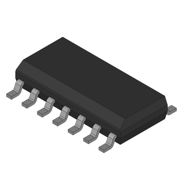
Renesas X40421S14-B
- Part No.:
- X40421S14-B
- Manufacturer:
- Renesas
- Category:
- Supervisors
- Package:
- 14-SOIC (0.154", 3.90mm Width)
- Datasheet:
-
 X40421S14-B.pdf
- Description:
- IC SUPERVISOR 2 CHANNEL 14SOIC
- Quantity:
- Payment:

- Shipping:

Inventory:773
Please send an inquiry. Send us your inquiry, and we will respond immediately.
Product details
Overview
X40421S14-B from Xicor is a dual-voltage CPU supervisor IC with integrated 4kbit EEPROM, battery backup switch, watchdog timer, and programmable reset thresholds. It monitors VCC (VTRIP1 = 4.6V ±1%) and V2MON (VTRIP2 = 2.6V ±2%), asserts active-low RESET on brownout or manual reset, delivers up to 50mA from VCC to VOUT, and supports I²C-compatible 400kHz 2-wire interface - used in network servers for SRAM retention during power fail.
For engineers reviewing the X40421S14-B datasheet, X40421S14-B pinout, X40421S14-B application, or X40421S14-B equivalent, key selection considerations include its dual-threshold voltage supervision, battery switchover hysteresis (±30mV), programmable power-on reset timeout (50/200/400/800ms), watchdog intervals (25ms/200ms/1.4s/off), and Block Lock™ EEPROM protection.
Technical Context
The X40421S14-B implements independent analog comparators for VTRIP1 and VTRIP2, with factory-set thresholds (4.6V/2.6V) reprogrammable down to 0.9V using high-voltage programming on WDO. Its reset logic generates an active-low open-drain RESET output valid down to VCC = 1V, with user-selectable tPURST delay and debounced MR input.
It integrates a system battery switch that connects VOUT to VCC (5Ω typical) above VTRIP1, and switches to VBATT (80Ω typical) when VCC drops below VBATT – 0.03V, with 60mV hysteresis. The 4kbit EEPROM uses Xicor's Direct Write™ cell (100k write cycles, 100-year retention) and supports 16-byte page writes with self-timed 5ms typical cycle time.
Key Specifications
| Parameter | Value and Actual Design Meaning |
|---|---|
| VTRIP1 | 4.6V ±1% - primary supply monitor threshold; holds RESET low until VCC exceeds this level and stabilizes for tPURST. |
| VTRIP2 | 2.6V ±2% - secondary monitor threshold; asserts V2FAIL when V2MON falls below this value. |
| tPURST | Selectable 50/200/400/800ms - determines minimum reset pulse width after power-up or manual reset release. |
| Watchdog interval | 25ms / 200ms / 1.4s / off - nonvolatile setting; WDO asserts low if SDA/SCL activity fails to restart timer within selected period. |
| VOUT drive capability | 5–50mA from VCC; 250µA from VBATT - powers external SRAM during main supply failure without external regulators. |
| EEPROM interface | 400kHz 2-wire (I²C-compatible) - supports standard slave address A0h; includes write protection via WP pin and Block Lock™. |
| Supply range | 2.7V to 5.5V - operates across industrial and computing rail voltages; standby current 6µA (watchdog off) or 25µA (watchdog on). |
Pinout & Package
Package: 14-lead SOIC (Small Outline Integrated Circuit) - surface-mount, 150mil body width, standard JEDEC MS-012AC footprint.
| Pin/Terminal | Circuit Role | Design Meaning |
|---|---|---|
| 1 V2FAIL | Open-drain voltage fail indicator | Asserts LOW when V2MON < VTRIP2; no power-up delay; requires external pull-up for logic HIGH. |
| 2 V2MON | Secondary voltage monitor input | Accepts unregulated or auxiliary supply; sets V2FAIL trip point; connect to VSS or VCC if unused. |
| 3 LOWLINE | Early low-VCC detect output | Open-drain signal goes LOW when VCC < VTRIP1; requires external pull-up resistor. |
| 4 WDO | Watchdog timeout output | Active-low open-drain; asserts when watchdog timer expires; used for high-voltage programming of VTRIPx. |
| 5 MR | Debounced manual reset input | Pull LOW to initiate system reset; internal weak pull-up; reset duration = tPURST after release. |
| 6 RESET | Active-low reset output | Open-drain; asserted during VCC brownout, MR assertion, or power-up until tPURST elapses. |
| 7 VSS | Ground reference | Primary return path for all internal circuits and I/O; must be low-impedance connection. |
| 8 SDA | Serial data bidirectional line | I²C-compatible; open-drain; requires external pull-up; used for EEPROM read/write and watchdog restart. |
| 9 SCL | Serial clock input | Master-generated clock; controls timing of all 2-wire interface transactions; no internal pull-up. |
| 10 WP | Hardware write protect | High = blocks all EEPROM and register writes; internal pull-down; overrides software lock bits. |
| 11 VBATT | Battery backup supply input | Provides backup power to VOUT and internal logic when VCC fails; connect to ground if unused. |
| 12 VOUT | System backup output | Switches between VCC and VBATT based on comparator thresholds and hysteresis; 0.1µF capacitor required. |
| 13 BATT-ON | Battery status indicator | CMOS HIGH when VOUT = VBATT; drives external PNP transistor for >50mA loads during normal operation. |
| 14 VCC | Main supply voltage input | 2.7–5.5V operating range; powers all internal functions except EEPROM write cycles (which use charge pump). |
Key Features
| Feature | Design Value |
|---|---|
| Dual programmable voltage monitoring | VTRIP1 and VTRIP2 thresholds adjustable down to 0.9V via high-voltage programming sequence - enables precision brownout detection for custom rails. |
| Battery-backed VOUT with hysteresis | Automatic switchover at VBATT ±30mV with 60mV total hysteresis - prevents oscillation during marginal supply transitions and ensures clean SRAM retention. |
| Nonvolatile control register | Stores WD1/WD0 (watchdog), PUP1/PUP0 (tPURST), and BP (block protect) bits across power cycles - eliminates boot-time configuration overhead. |
| Block Lock™ EEPROM protection | Hardware + software write protection: WP pin disables all writes; BP bit locks upper 256 bytes (100h–1FFh) - prevents accidental corruption of critical firmware parameters. |
| Fault Detection Register (FDR) | Volatile 8-bit register (address 0FFh) captures cause of last reset - LV1F/LV2F/WDF/MRF bits identify brownout, power fail, or watchdog timeout for diagnostics. |
Applications
| Network Server Power Management | Rack-Mount Industrial Controller |
|---|---|
|
Use Scenario: Maintains SRAM contents and logs fault events during AC mains interruption in dual-power-supply server chassis. IC Role / Device Role / Timing Role: Dual-voltage supervisor asserts RESET on 5V rail collapse while switching VOUT to 3.3V battery to sustain memory; FDR records LV1F flag for root-cause analysis. Use Value: Enables graceful shutdown and post-failure diagnostics without external supervisors or discrete logic, reducing BOM count by one IC. |
Use Scenario: Monitors both 24V field bus supply and 5V logic rail in PLC backplane, triggering safe state transition on undervoltage. IC Role / Device Role / Timing Role: V2MON tracks 24V via resistor divider; VTRIP2 set to 20.5V; LOWLINE signals early warning 100ms before full shutdown. Use Value: Provides deterministic response to partial supply degradation - avoids spurious resets from transient dips while ensuring fail-safe behavior. |
| Desktop PC BIOS Protection | Telecom Line Card Supervision |
|
Use Scenario: Secures UEFI variable storage in desktop motherboard, preventing corruption during unstable 3.3V standby rail conditions. IC Role / Device Role / Timing Role: EEPROM stores boot configuration; WP pin hardwired HIGH during manufacturing; Block Lock™ protects top 256 bytes containing recovery keys. Use Value: Eliminates need for separate SPI flash with hardware write protect, cutting PCB area and routing complexity for compact ATX layouts. |
Use Scenario: Supervises redundant -48V DC feeds and +3.3V logic in carrier-grade line card, asserting WDO if microcontroller hangs during firmware update. IC Role / Device Role / Timing Role: Watchdog timer set to 200ms; SDA activity monitored during update sequence; WDO triggers hardware reset if host misses two consecutive restart pulses. Use Value: Guarantees automatic recovery from hung states without operator intervention - meets ITU-T Y.1731 availability requirements (>99.999%). |
Equivalent & Alternatives
The following parts are listed as comparable options for similar dual-voltage supervisor with EEPROM applications.
| Alternative Part | Technical Difference | Application Difference | Selection Advice |
|---|---|---|---|
| MAX6821EUK+T | Single 2.93V reset threshold; no V2MON input; 1kbit EEPROM; 100kHz I²C only | Lacks secondary voltage monitoring and programmable VTRIP2; suitable only for single-rail systems requiring basic reset + small memory | Select when cost sensitivity outweighs dual-monitoring requirement and EEPROM size < 2kbit suffices. |
| TPS3823MPW | Triple voltage monitor (3 thresholds); no EEPROM; push-pull RESET; 2.5–5.5V supply | Provides three independent reset sources but zero nonvolatile storage; requires external serial memory for parameter retention | Choose when multi-rail validation (e.g., 12V/5V/3.3V) is mandatory and EEPROM functionality is handled separately. |
Compared with MAX6821EUK+T and TPS3823MPW, the X40421S14-B uniquely integrates dual-programmable voltage supervision, battery switchover, watchdog, and 4kbit protected EEPROM in a single 14-pin SOIC - eliminating four discrete components while enabling autonomous fault logging and SRAM backup without layout redesign.
Availability
X40421S14-B is available at Aetrix Electronics and suitable for network servers, industrial PLCs, and telecom line cards requiring stable component supply, long-term EEPROM data retention, and deterministic power-fail response.
Supply support for X40421S14-B includes scheduled delivery planning, volume procurement assistance, BOM continuity management, traceable sourcing, and lifecycle availability coordination for OEM customers, industrial embedded developers, connected-device designers, and electronics production programs.
Manufacturer
Xicor Inc. was a fabless semiconductor company specializing in nonvolatile memory and power management ICs, acquired by Intersil in 2001 and later by Renesas Electronics. Known for innovation in EEPROM architecture and integrated supervisors.
The X40420/X40421 family was designed to consolidate power-on reset, voltage monitoring, watchdog, and memory into one die - targeting space-constrained computing and communications systems needing high reliability and minimal external components.
FAQ
What is the factory-default VTRIP1 and VTRIP2 for X40421S14-B?
The X40421S14-B ships with factory-programmed thresholds of 4.6V ±1% for VTRIP1 and 2.6V ±2% for VTRIP2, corresponding to the "-B" suffix. These values remain stable over temperature and time unless reprogrammed using the high-voltage VTRIPx programming sequence defined in the datasheet.
Does X40421S14-B support I²C standard addressing and ACK/NACK protocol?
Yes, X40421S14-B uses standard I²C slave address A0h (10100000b) and fully complies with I²C ACK/NACK timing. It acknowledges the slave address byte when the device ID matches, responds with ACK after each data byte in write mode, and transmits data with ACK polling in read mode - compatible with standard I²C masters.
How does the battery switchover hysteresis work in X40421S14-B?
X40421S14-B implements 60mV total hysteresis around the VBATT switchover point: VOUT switches from VCC to VBATT when VCC falls below VBATT – 0.03V, and switches back to VCC only when VCC rises above VBATT + 0.03V - preventing oscillation during slow supply recovery or noisy transitions.
Can X40421S14-B's EEPROM be written while VCC is below 2.7V?
No. X40421S14-B requires VCC ≥ 2.7V to perform EEPROM writes. Although RESET remains valid down to VCC = 1V, the internal charge pump for programming cannot operate below the 2.7V minimum supply specification - write attempts below this voltage will not be acknowledged.
What is the purpose of the BATT-ON pin on X40421S14-B?
The BATT-ON pin on X40421S14-B is a CMOS output that goes HIGH when VOUT is sourced from VBATT, indicating battery backup mode. It is intended to drive an external PNP pass transistor, enabling >50mA load currents during normal VCC-powered operation while automatically disabling the transistor during battery fallback.
X40421S14-B Specifications
- Product attributes
- Attribute value
- Manufacturer:
- Renesas
- Series:
- -
- Package/Case:
- 14-SOIC (0.154", 3.90mm Width)
- Packaging:
- Bulk
- Product Status:
- Obsolete
- Programmable:
- Not Verified
- Type:
- Multi-Voltage Supervisor
- Number of Voltages Monitored:
- 2
- Voltage - Threshold:
- 2.6V, 4.6V
- Output:
- Open Drain or Open Collector
- Reset:
- Active Low
- Reset Timeout:
- Adjustable/Selectable
- Operating Temperature:
- 0°C ~ 70°C (TA)
- Grade:
- -
- Qualification:
- -
- Mounting Type:
- Surface Mount
- Supplier Device Package:
- 14-SOIC
X40421S14-B FAQ
1.How can I place an order for X40421S14-B through Aetrix?
Please submit a Request for Quotation (RFQ) for X40421S14-B on Aetrix. Our sales agent will provide a competitive quotation and guide you through the order confirmation once you accept the terms.
2.Are the price and stock information for X40421S14-B reliable?
The price and inventory of X40421S14-B are updated periodically and may fluctuate due to market conditions. Stock and pricing data are typically refreshed every 24 hours. Quotation validity for X40421S14-B is usually 5 days.
3.What payment methods are accepted for X40421S14-B?
We accept Wire Transfer, PayPal, Credit Card, Western Union, MoneyGram, and Escrow for X40421S14-B transactions.
Note: Certain payment methods may incur a processing fee.
4.How is shipping managed for X40421S14-B?
X40421S14-B orders can be shipped via leading logistics carriers, including DHL, UPS, FedEx, TNT, or Registered Mail.
Once your X40421S14-B order is processed, you will receive an email with the shipment details and tracking number.
Note: Tracking information may take up to 24 hours to appear. Express delivery typically takes 3–5 business days.
5.How can I obtain technical support or documentation for X40421S14-B?
For technical support, including X40421S14-B datasheets, pinout diagrams, or application guidance, please contact our engineering support team. They can provide detailed documentation and assistance for your X40421S14-B requirements.
6.How does Aetrix verify that X40421S14-B is sourced from the original manufacturer or authorized distributors?
All X40421S14-B products on Aetrix are procured from qualified distributors and authorized channels. Our dedicated quality assurance team conducts strict verification, including traceability checks and, if necessary, third-party testing. This ensures that X40421S14-B meets industry standards.
7.What is the process for return or replacement of X40421S14-B?
All X40421S14-B units undergo pre-shipment inspection (PSI). If there is an issue with X40421S14-B, returns or replacements are accepted under the following conditions:
1.Quantity discrepancies, incorrect items, or visible external defects (such as breakage or corrosion), acknowledged by Aetrix.
2.The issue is reported within 90 days of delivery.
3.The X40421S14-B part is unused and in its original packaging.
Return procedure for X40421S14-B:
1.Submit a request within 90 days.
2.Obtain a Return Material Authorization (RMA) from Aetrix.
X40421S14-B Tags
-
MIC826SYMT-TR
Microchip Technology

-
APX803S-31SA-7
Diodes Incorporated
-
APX803L20-29SA-7
Diodes Incorporated

-
TPS3828-33DBVR
Texas Instruments

-
V6340RSP3B+
EM Microelectronic
-
EM6325CXSP5B-2.9+
EM Microelectronic
-
MCP120T-300I/TT
Microchip Technology
-
MCP130T-315I/TT
Microchip Technology
-
MCP120T-475I/TT
Microchip Technology
-
MCP111T-300E/TT
Microchip Technology
-
MCP120T-315I/TT
Microchip Technology
-
MCP809T-315I/TT
Microchip Technology
Tech Hub

TTL and CMOS logic families differ in thresholds, loading, output drive, power and timing. This engineering guide compares 74HC and 74HCT, calculates noise margins and checks 3.3 V/5 V compatibility.

A practical engineering guide to 3.3V and 5V logic compatibility, input thresholds, resistor dividers, translator ICs, MOSFET level shifting, I2C pull-ups, timing limits and power-sequencing risks.

The 74HC595 uses push-pull logic outputs, while the TPIC6B595 uses 50 V open-drain DMOS sinks for higher-power loads. This guide compares timing, current limits, 3.3 V interfacing, load wiring, thermal…

The 74HC595 converts serial data into eight stable parallel outputs. This guide covers pin functions, shift and storage timing, OE and MR behavior, drive-current limits, cascading, voltage compatibilit…

A technical comparison of level-sensitive latches and edge-triggered flip-flops, covering timing windows, setup and hold limits, master–slave operation, time borrowing, race-through, HDL inference and…

A D latch stores one bit while Enable controls when data can pass. This reference covers gate-level operation, truth tables, transparency, setup and hold timing, LE versus OE, common ICs and practical …

An SR latch stores one bit through cross-coupled feedback. This engineering reference covers NOR and NAND implementations, truth tables, forbidden-state recovery, gated operation, switch debouncing, fa…

Latch circuits retain one bit through feedback. This technical reference covers SR and D latches, truth tables, transparency, timing limits, latch-versus-flip-flop behavior, applications and common log…

An engineering guide to LED driver operation, constant-current and constant-voltage outputs, linear and switching topologies, dimming, IC selection, calculations, replacement compatibility, and fault c…

Operational amplifier guide covering op amp basics, feedback, ideal vs real op amps, common configurations, buffer circuits, offset, bias current, gain-bandwidth, slew rate, rail-to-rail limits and sel…


