
 My Inquiry
 My Account


Renesas X9418WP24-2.7
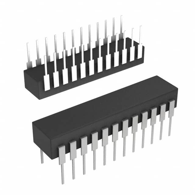
- Part No.:
- X9418WP24-2.7
- Manufacturer:
- Renesas
- Category:
- Digital Potentiometers
- Package:
- 24-DIP (0.600", 15.24mm)
- Datasheet:
-
 X9418WP24-2.7.pdf
- Description:
- IC DGTL POT 10KOHM 64TAP 24DIP
- Quantity:
- Payment:

- Shipping:

Inventory:3,335
Please send an inquiry. Send us your inquiry, and we will respond immediately.
Product details
Overview
X9418WP24-2.7 from Intersil is a dual digitally controlled potentiometer (XDCP™) with 2-wire I²C-compatible interface, 64-tap resolution per pot, 10kΩ end-to-end resistance, ±2.7V to ±5.5V analog supply range (V+/V−), and 2.7V–5.5V digital supply (VCC). It operates across –40°C to +85°C in a 24-pin PDIP package and is used for precision offset adjustment in industrial sensor signal conditioning.
For engineers reviewing the X9418WP24-2.7 datasheet, X9418WP24-2.7 pinout, X9418WP24-2.7 application, or X9418WP24-2.7 equivalent, key selection criteria include dual-potentiometer integration, nonvolatile wiper position storage (DR0 auto-load at power-up), hardware write protection (WP pin), low standby current (<1µA), and compatibility with battery-powered or wide-voltage analog systems requiring ratiometric stability.
Technical Context
The X9418WP24-2.7 implements two independent 63-segment resistor arrays with CMOS-switched wipers controlled by 6-bit volatile Wiper Counter Registers (WCRs). Each potentiometer features four 6-bit nonvolatile Data Registers (DR0–DR3) supporting direct read/write, transfer to/from WCR, and global register operations via I²C.
Its 2-wire serial interface supports standard-mode (400kHz max) timing, device addressing via A0–A3 (16-device bus capacity), and hardware write protection via active-low WP pin. Power-up behavior loads DR0 into both WCRs, ensuring deterministic initial wiper positions without host intervention.
Key Specifications
| Parameter | Value and Actual Design Meaning |
|---|---|
| End-to-end resistance | 10kΩ ±20% - defines full-scale voltage division ratio and load interaction in feedback networks |
| Resolution | 64 taps (6-bit) - enables 1.56% step granularity for fine gain/offset tuning |
| Analog supply range (V+/V−) | ±2.7V to ±5.5V - supports bipolar signal paths including op-amp inputs and comparator hysteresis circuits |
| Digital supply (VCC) | 2.7V to 5.5V - ensures interoperability with 3.3V and 5V microcontrollers without level shifting |
| Standby current | <1µA - extends battery life in portable instrumentation and remote sensors |
| Nonvolatile endurance | 100,000 data changes per bit - guarantees long-term reliability in field-updatable calibration systems |
| Data retention | 100 years - preserves factory or field calibration settings across product lifetime |
Pinout & Package
Package: 24-pin plastic DIP (dual in-line package), 0.600" width, JEDEC MS-001 compliant, lead spacing 0.100", RoHS-compliant (Pb-free plus anneal).
| Pin/Terminal | Circuit Role | Design Meaning |
|---|---|---|
| VCC | Digital system supply | Power source for I²C interface logic and control circuitry; must be stable before V+/V− |
| VSS | Digital ground reference | Common return path for SCL, SDA, address, and WP signals; isolated from analog ground |
| V+, V− | Analog supply rails | Provide bias for resistor arrays and wiper switches; define full analog operating range (±2.7V to ±5.5V) |
| SCL, SDA | I²C serial bus interface | Open-drain bidirectional lines requiring external pull-ups; support up to 400kHz clock rate |
| A0–A3 | Device address inputs | Set LSBs of 8-bit slave address (0101xxxx); enable up to 16 devices on shared bus |
| WP | Hardware write protect | Active-low input disabling nonvolatile writes to DR0–DR3; prevents accidental calibration overwrite |
| VH0/RH0, VL0/RL0, VW0/RW0 | Potentiometer 0 terminals | High-side, low-side, and wiper connections for first 10kΩ array; electrically equivalent to mechanical pot pins |
| VH1/RH1, VL1/RL1, VW1/RW1 | Potentiometer 1 terminals | High-side, low-side, and wiper connections for second 10kΩ array; fully independent of Pot 0 |
| NC | No connection | Pins 11, 15, 18, 19, 21, 22, 23 - internally unconnected; must remain floating or grounded per layout best practice |
Key Features
| Feature | Design Value |
|---|---|
| Dual independent potentiometers | Two 10kΩ, 64-tap arrays on one die eliminate board space and BOM count vs. discrete solutions |
| Nonvolatile wiper storage | Four 6-bit Data Registers per pot retain calibration values across power cycles; DR0 auto-loads at startup |
| Hardware write protection | WP pin disables EEPROM writes independently of software control-critical for field-deployed recalibration safety |
| Low-power standby mode | <1µA ICC standby current enables always-on sensor front-ends without compromising battery runtime |
| Bipolar analog operation | V+/V− rails support ±2.7V to ±5.5V operation-enables use in AC-coupled, rail-to-rail, and dual-supply op-amp circuits |
Applications
| Instrumentation Offset Calibration | Programmable Gain Amplifier |
|---|---|
Use Scenario: Zeroing DC offset in precision thermocouple or strain gauge amplifiers during factory calibration and field maintenance. IC Role / Device Role / Timing Role: Dual-potentiometer provides independent null adjustment for differential input stage and output offset trim. Use Value: Eliminates manual trimpots; enables automated calibration via MCU I²C, reducing test time and improving repeatability over temperature. | Use Scenario: Setting closed-loop gain in programmable instrumentation amplifiers used in data acquisition modules. IC Role / Device Role / Timing Role: One potentiometer configures feedback resistor ratio (R2/R1) in noninverting amplifier topology. Use Value: Enables dynamic gain switching under firmware control-supports multi-range measurement without hardware change. |
| Voltage Reference Adjustment | Comparator Hysteresis Control |
Use Scenario: Fine-tuning output voltage of adjustable LDOs or bandgap references in power management ICs. IC Role / Device Role / Timing Role: Acts as two-terminal variable resistor in feedback divider network of TL317-type regulators. Use Value: Permits post-manufacturing voltage binning and field recalibration without soldering-improves yield and serviceability. | Use Scenario: Configuring hysteresis window in window comparators for threshold detection in motor control or battery monitoring. IC Role / Device Role / Timing Role: Sets upper/lower trip points using dual potentiometers in resistor-divider networks feeding comparator inputs. Use Value: Allows adaptive hysteresis tuning via host MCU-prevents chatter in noisy environments while maintaining fast response. |
Equivalent & Alternatives
The following parts are listed as comparable options for similar digitally controlled potentiometer applications.
| Alternative Part | Technical Difference | Application Difference | Selection Advice |
|---|---|---|---|
| AD5242BRUZ10 | Single 10kΩ pot, I²C interface, 256-tap resolution, 2.7–5.5V supply, no V+/V− rails | Lacks bipolar analog capability; requires external op-amp for bipolar signal conditioning | Select when only unipolar adjustment is needed and higher resolution justifies single-pot limitation |
| MCP41HV51-103 | Dual 10kΩ pots, SPI interface, 256-tap, 4.5–18V analog supply, no nonvolatile memory | No DR0 auto-load at power-up; requires host initialization; supports higher analog voltages | Select for high-voltage analog systems (>±5.5V) where SPI is preferred and calibration persistence is managed externally |
Compared with AD5242BRUZ10 and MCP41HV51-103, the X9418WP24-2.7 uniquely combines dual-pot integration, bipolar V+/V− operation, nonvolatile DR0 auto-load, and hardware write protection-making it optimal for industrial sensor signal chains requiring robust, self-initializing analog trimming.
Availability
X9418WP24-2.7 is available at Aetrix Electronics and suitable for industrial sensor calibration, programmable power supplies, and test equipment requiring stable component supply with guaranteed long-term availability and traceable sourcing.
Supply support for X9418WP24-2.7 includes scheduled delivery planning, volume procurement assistance, BOM continuity management, traceable sourcing, and lifecycle availability coordination for OEM customers, industrial embedded developers, connected-device designers, and electronics production programs.
Manufacturer
Intersil Corporation (now part of Renesas Electronics) designs high-performance analog and mixed-signal ICs for industrial, aerospace, and communications markets.
The X9418 family delivers digitally controlled potentiometers optimized for precision analog trimming in harsh environments-emphasizing nonvolatile storage, wide supply tolerance, and hardware-level write protection.
FAQ
What is the power-up behavior of the X9418WP24-2.7?
At power-up, the X9418WP24-2.7 automatically loads the contents of Data Register 0 (DR0) into both Wiper Counter Registers (WCRs), establishing deterministic initial wiper positions without host intervention. This requires proper sequencing: VCC must stabilize first, followed by V+ and V−, then potentiometer pins (VH/VL/VW). The X9418WP24-2.7 will not complete recall until all three supplies reach final value.
Does the X9418WP24-2.7 support true bipolar analog operation?
Yes, the X9418WP24-2.7 supports true bipolar analog operation via dedicated V+ and V− pins rated from ±2.7V to ±5.5V. This allows the resistor arrays to function across negative and positive voltages-enabling use in AC-coupled signal paths, dual-supply op-amps, and comparator hysteresis circuits where mechanical potentiometers would require external level-shifting.
How does the hardware write protect (WP) pin function on the X9418WP24-2.7?
The WP pin on the X9418WP24-2.7 is an active-low input that disables all nonvolatile writes to the Data Registers (DR0–DR3) when asserted. When WP = LOW, commands like "Write Data Register" or "XFR WCR to DR" are ignored-even if valid I²C traffic is received. This provides fail-safe protection against accidental calibration overwrite during field updates or firmware glitches.
What is the maximum I²C clock frequency supported by the X9418WP24-2.7?
The X9418WP24-2.7 supports standard-mode I²C operation up to 400kHz, with guaranteed timing parameters including tCYC ≥ 2500ns, tHIGH ≥ 600ns, and tLOW ≥ 1300ns. It uses open-drain SCL/SDA pins requiring external pull-up resistors; recommended values depend on bus capacitance but typically range from 1.8kΩ (100pF) to 4.7kΩ (20pF) for reliable 400kHz operation.
Can the X9418WP24-2.7 be used as a two-terminal variable resistor?
Yes, the X9418WP24-2.7 can be configured as a two-terminal variable resistor by connecting either VH/RH or VL/RL to the wiper VW/RW, leaving the unused terminal open or tied to a fixed potential. This configuration is commonly used in current-setting applications (e.g., LED driver bias) and programmable current sources-leveraging the same 64-tap resolution and nonvolatile storage as the three-terminal potentiometer mode.
X9418WP24-2.7 Specifications
- Product attributes
- Attribute value
- Manufacturer:
- Renesas
- Series:
- XDCP™
- Package/Case:
- 24-DIP (0.600", 15.24mm)
- Packaging:
- Tube
- Product Status:
- Obsolete
- Programmable:
- Not Verified
- Taper:
- Linear
- Configuration:
- Potentiometer
- Number of Circuits:
- 2
- Number of Taps:
- 64
- Resistance (Ohms):
- 10k
- Interface:
- I2C
- Memory Type:
- Non-Volatile
- Voltage - Supply:
- ±2.7V ~ 5.5V
- Features:
- Selectable Address
- Tolerance:
- ±20%
- Temperature Coefficient (Typ):
- ±300ppm/°C
- Mounting Type:
- Through Hole
- Grade:
- -
- Qualification:
- -
- Supplier Device Package:
- 24-PDIP
- Operating Temperature:
- 0°C ~ 70°C
- Resistance - Wiper (Ohms) (Typ):
- 150
X9418WP24-2.7 FAQ
1.How can I place an order for X9418WP24-2.7 through Aetrix?
Please submit a Request for Quotation (RFQ) for X9418WP24-2.7 on Aetrix. Our sales agent will provide a competitive quotation and guide you through the order confirmation once you accept the terms.
2.Are the price and stock information for X9418WP24-2.7 reliable?
The price and inventory of X9418WP24-2.7 are updated periodically and may fluctuate due to market conditions. Stock and pricing data are typically refreshed every 24 hours. Quotation validity for X9418WP24-2.7 is usually 5 days.
3.What payment methods are accepted for X9418WP24-2.7?
We accept Wire Transfer, PayPal, Credit Card, Western Union, MoneyGram, and Escrow for X9418WP24-2.7 transactions.
Note: Certain payment methods may incur a processing fee.
4.How is shipping managed for X9418WP24-2.7?
X9418WP24-2.7 orders can be shipped via leading logistics carriers, including DHL, UPS, FedEx, TNT, or Registered Mail.
Once your X9418WP24-2.7 order is processed, you will receive an email with the shipment details and tracking number.
Note: Tracking information may take up to 24 hours to appear. Express delivery typically takes 3–5 business days.
5.How can I obtain technical support or documentation for X9418WP24-2.7?
For technical support, including X9418WP24-2.7 datasheets, pinout diagrams, or application guidance, please contact our engineering support team. They can provide detailed documentation and assistance for your X9418WP24-2.7 requirements.
6.How does Aetrix verify that X9418WP24-2.7 is sourced from the original manufacturer or authorized distributors?
All X9418WP24-2.7 products on Aetrix are procured from qualified distributors and authorized channels. Our dedicated quality assurance team conducts strict verification, including traceability checks and, if necessary, third-party testing. This ensures that X9418WP24-2.7 meets industry standards.
7.What is the process for return or replacement of X9418WP24-2.7?
All X9418WP24-2.7 units undergo pre-shipment inspection (PSI). If there is an issue with X9418WP24-2.7, returns or replacements are accepted under the following conditions:
1.Quantity discrepancies, incorrect items, or visible external defects (such as breakage or corrosion), acknowledged by Aetrix.
2.The issue is reported within 90 days of delivery.
3.The X9418WP24-2.7 part is unused and in its original packaging.
Return procedure for X9418WP24-2.7:
1.Submit a request within 90 days.
2.Obtain a Return Material Authorization (RMA) from Aetrix.
X9418WP24-2.7 Tags
-
MCP4018T-103E/LT
Microchip Technology
-
MCP4018T-503E/LT
Microchip Technology

-
MCP4011T-103E/SN
Microchip Technology
-
MCP4018T-104E/LT
Microchip Technology
-
MCP4017T-503E/LT
Microchip Technology
-
MCP4018T-502E/LT
Microchip Technology
-
MCP4017T-103E/LT
Microchip Technology

-
MCP4531T-103E/MF
Microchip Technology
-
MCP4021T-202E/SN
Microchip Technology

-
MCP4023T-103E/CH
Microchip Technology
-
MCP4022T-503E/CH
Microchip Technology

-
MCP4551T-502E/MS
Microchip Technology
Tech Hub

A practical engineering and sourcing framework covering lifecycle verification, lifetime-buy calculations, replacement qualification, supplier checks and counterfeit-risk controls.

TTL and CMOS logic families differ in thresholds, loading, output drive, power and timing. This engineering guide compares 74HC and 74HCT, calculates noise margins and checks 3.3 V/5 V compatibility.

A practical engineering guide to 3.3V and 5V logic compatibility, input thresholds, resistor dividers, translator ICs, MOSFET level shifting, I2C pull-ups, timing limits and power-sequencing risks.

The 74HC595 uses push-pull logic outputs, while the TPIC6B595 uses 50 V open-drain DMOS sinks for higher-power loads. This guide compares timing, current limits, 3.3 V interfacing, load wiring, thermal…

The 74HC595 converts serial data into eight stable parallel outputs. This guide covers pin functions, shift and storage timing, OE and MR behavior, drive-current limits, cascading, voltage compatibilit…

A technical comparison of level-sensitive latches and edge-triggered flip-flops, covering timing windows, setup and hold limits, master–slave operation, time borrowing, race-through, HDL inference and…

A D latch stores one bit while Enable controls when data can pass. This reference covers gate-level operation, truth tables, transparency, setup and hold timing, LE versus OE, common ICs and practical …

An SR latch stores one bit through cross-coupled feedback. This engineering reference covers NOR and NAND implementations, truth tables, forbidden-state recovery, gated operation, switch debouncing, fa…

Latch circuits retain one bit through feedback. This technical reference covers SR and D latches, truth tables, transparency, timing limits, latch-versus-flip-flop behavior, applications and common log…

An engineering guide to LED driver operation, constant-current and constant-voltage outputs, linear and switching topologies, dimming, IC selection, calculations, replacement compatibility, and fault c…


