
 My Inquiry
 My Account


Renesas X95820UV14I-2.7T1
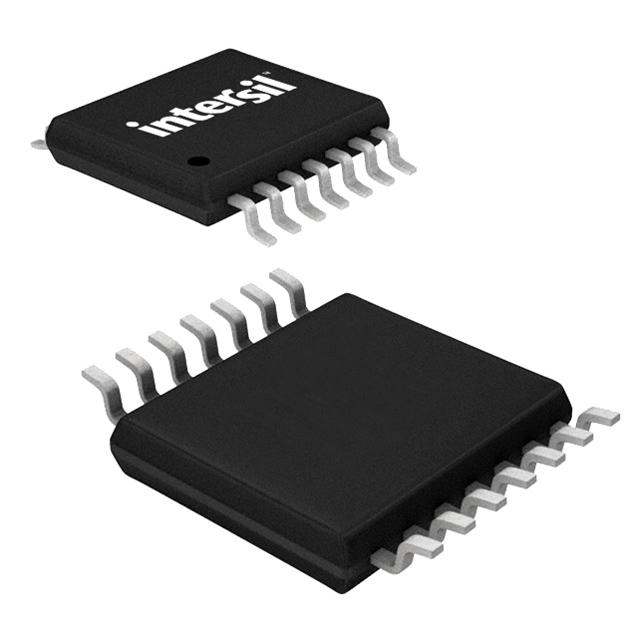
- Part No.:
- X95820UV14I-2.7T1
- Manufacturer:
- Renesas
- Category:
- Digital Potentiometers
- Package:
- 14-TSSOP (0.173", 4.40mm Width)
- Datasheet:
-
 X95820UV14I-2.7T1.pdf
- Description:
- IC DGT POT 50KOHM 256TAP 14TSSOP
- Quantity:
- Payment:

- Shipping:

Inventory:2,191
Please send an inquiry. Send us your inquiry, and we will respond immediately.
Product details
Overview
X95820UV14I-2.7T1 from Intersil is a dual digital controlled potentiometer (XDCP™) IC implementing two independent 256-tap, 50kΩ CMOS resistor networks with I²C interface, wiper registers, and non-volatile initial value storage-used for precision analog voltage division and rheostat control in programmable gain amplifiers, sensor calibration, and DC bias adjustment circuits.
For engineers reviewing the X95820UV14I-2.7T1 datasheet, X95820UV14I-2.7T1 pinout, X95820UV14I-2.7T1 application, or X95820UV14I-2.7T1 equivalent, key selection criteria include I²C address configurability (A0–A2), 2.7V–5.5V supply range, 70Ω typical wiper resistance at 3.3V, ±0.5 LSB differential nonlinearity in voltage divider mode, and industrial temperature operation (−40°C to +85°C).
Technical Context
The X95820UV14I-2.7T1 integrates two monolithic DCPs sharing a single I²C slave interface with hardware write protection (WP), three address pins (A0–A2), and separate RH/RL/RW terminals per channel. Each DCP uses resistor ladder + CMOS switch architecture controlled by an 8-bit volatile Wiper Register (WR) and backed by a non-volatile Initial Value Register (IVR) that loads on power-up.
It operates in two primary modes: voltage divider (RH→VCC, RL→GND, RW→output) and rheostat (RW–RL or RW–RH). Wiper position updates occur within 1 µs of SCL falling edge, and non-volatile writes require 12–20 ms with automatic recall at VCC ≥ 1.8 V. Standby current is <5 µA at 5.5 V.
Key Specifications
| Parameter | Value and Actual Design Meaning |
|---|---|
| Total Resistance | 50 kΩ per DCP - sets full-scale voltage division ratio and rheostat impedance range. |
| Resolution | 256 taps (0.4% step size) - enables fine-grained analog tuning with 8-bit digital control. |
| Wiper Resistance | 70 Ω typical @ 3.3 V - minimizes signal path error and loading in high-impedance feedback networks. |
| I²C Interface | Standard-mode (400 kHz), 3 address pins → up to 8 devices/bus - supports multi-pot systems without bus contention. |
| Non-volatile Storage | 150,000 write cycles, 50-year data retention @ ≤75°C - ensures reliable power-on default settings across product lifetime. |
| Operating Voltage | 2.7 V to 5.5 V - compatible with 3.3 V and 5 V logic/system rails without level shifting. |
| Temperature Range | −40°C to +85°C (industrial) - validated for embedded control and instrumentation environments. |
Pinout & Package
Package: 14-lead TSSOP (Thin Shrink Small Outline Plastic), RoHS-compliant, Pb-free plus anneal finish, body dimensions 4.95 mm × 6.25 mm × 1.05 mm max height.
| Pin/Terminal | Circuit Role | Design Meaning |
|---|---|---|
| 1 (VCC) | Power supply input | Supplies core logic and DCP array; must be decoupled near pin with 0.1 µF ceramic capacitor. |
| 2 (WP) | Hardware write protect | Active-low; disables all I²C writes when pulled low-prevents accidental register corruption during system reset or noise events. |
| 3 (RH0), 4 (RL0), 5 (RW0) | DCP0 high/low/wiper terminals | Form first 3-terminal potentiometer or 2-terminal variable resistor; RH0 and RL0 define end-to-end resistance; RW0 provides adjustable tap point. |
| 6 (A2), 13 (A0), 14 (A1) | I²C device address inputs | Set 3-bit slave address (1010 A2 A1 A0 R/W); enable up to eight X95820 devices on same bus without software arbitration. |
| 7 (SCL), 8 (SDA) | I²C clock and bidirectional data | Compliant with standard-mode timing (tLOW = 1300 ns, tHIGH = 600 ns); require external pull-ups (2–20 kΩ depending on bus capacitance). |
| 9 (GND) | Analog/digital ground reference | Common return for VCC, DCP terminals, and I²C signals; must be low-impedance connection to system ground plane. |
| 10 (RW1), 11 (RL1), 12 (RH1) | DCP1 high/low/wiper terminals | Independent second potentiometer with identical electrical behavior to DCP0; enables dual-channel gain/bias control in single package. |
Key Features
| Feature | Design Value |
|---|---|
| Dual 256-tap DCPs in one IC | Reduces board space and BOM count vs. discrete pots or two single-channel ICs; enables matched performance between channels (±2 LSB wiper voltage matching). |
| Volatile WR + non-volatile IVR per DCP | Allows runtime tuning (WR) while preserving factory- or user-programmed startup state (IVR); eliminates need for external EEPROM or MCU initialization code. |
| Low 70 Ω typical wiper resistance | Minimizes insertion loss and THD in audio and precision signal paths; maintains linearity under load in op-amp feedback configurations. |
| Industrial-grade reliability | 150,000 endurance cycles and 50-year data retention ensure long-term stability in unattended equipment such as medical sensors or industrial controllers. |
| Hardware WP pin + I²C protocol safeguards | Prevents unintended writes during power transients or firmware glitches-critical for safety-critical biasing and calibration functions. |
Applications
| Programmable Gain Amplifier | Sensor Offset Calibration |
|---|---|
Use Scenario: Adjusting feedback network resistance in instrumentation amplifier to select gain from 1× to 100× via microcontroller. IC Role / Device Role / Timing Role: Dual DCP acts as digitally reconfigurable resistor divider in both gain-setting and reference-bias paths. Use Value: Enables software-selectable gain without relays or manual trimmers; 50 kΩ resistance matches common op-amp input impedance requirements. | Use Scenario: Compensating thermal drift in bridge-based pressure or strain sensors by adjusting null voltage before ADC input. IC Role / Device Role / Timing Role: One DCP serves as precision offset nulling pot in Wheatstone bridge output stage; second used for span calibration. Use Value: Achieves <±0.1% full-scale offset correction using 256-step resolution and monotonic DNL ≤±0.5 LSB. |
| DC Bias Adjustment | Audio Volume Control |
Use Scenario: Setting quiescent current in Class-AB audio output stage or bias point in RF front-end LNA. IC Role / Device Role / Timing Role: Rheostat-mode DCP (RW–RL) replaces mechanical preset for stable, repeatable DC current control. Use Value: Eliminates mechanical wear and environmental drift; 70 Ω wiper resistance avoids distortion in high-gain bias loops. | Use Scenario: Implementing mute-ramp and channel-balanced volume control in consumer audio DAC output stage. IC Role / Device Role / Timing Role: Dual DCPs operate in voltage-divider mode to attenuate left/right analog audio signals independently. Use Value: Provides glitch-free, monotonic attenuation with <1 µs wiper response and matched tracking (±2 LSB) between channels. |
Equivalent & Alternatives
The following parts are listed as comparable options for similar digital potentiometer applications.
| Alternative Part | Technical Difference | Application Difference | Selection Advice |
|---|---|---|---|
| AD5242BRUZ10 | Single 256-tap, 10 kΩ DCP; I²C interface; no hardware WP pin; 16-lead TSSOP. | Lacks dual-channel integration and write-protection pin; requires two units for dual-channel use. | Select when only one pot is needed and board space allows larger 16-pin footprint. |
| MCP45HV51-503E/ST | Dual 256-tap, 50 kΩ DCP; SPI interface; 14-lead TSSOP; 5.5 V max supply; no non-volatile IVR. | Requires SPI host instead of I²C; lacks power-on recall-needs MCU initialization on every boot. | Choose for SPI-based systems where deterministic timing and absence of I²C arbitration is preferred. |
Compared with AD5242BRUZ10 and MCP45HV51-503E/ST, the X95820UV14I-2.7T1 uniquely delivers dual-channel I²C control with hardware write protection and guaranteed power-on default values-reducing firmware overhead and improving system robustness in industrial calibration and programmable analog interfaces.
Availability
X95820UV14I-2.7T1 is available at Aetrix Electronics and suitable for programmable gain amplifiers, sensor calibration modules, DC bias adjustment circuits, and audio volume control systems requiring stable component supply and long-term parametric consistency.
Supply support for X95820UV14I-2.7T1 includes scheduled delivery planning, volume procurement assistance, BOM continuity management, traceable sourcing, and lifecycle availability coordination for OEM customers, industrial embedded developers, connected-device designers, and electronics production programs.
Manufacturer
Intersil Corporation (now part of Renesas Electronics) designs high-performance analog and mixed-signal ICs for precision power management, interface, and signal conditioning applications.
The X95820 series was developed specifically for digitally reconfigurable analog signal paths in industrial, test & measurement, and medical instrumentation-emphasizing non-volatile configuration retention, low wiper resistance, and I²C simplicity.
FAQ
What is the power-on behavior of the X95820UV14I-2.7T1?
At power-up, the X95820UV14I-2.7T1 recalls the contents of its two non-volatile Initial Value Registers (IVRs) into the corresponding volatile Wiper Registers (WRs), placing both wipers at their stored positions. This occurs after VCC exceeds 1.8 V and completes within 3 ms. The default IVR value is 0x80 (mid-scale), so wipers start centered unless previously programmed.
Does the X95820UV14I-2.7T1 support true dual-channel synchronization?
Yes-the X95820UV14I-2.7T1 allows simultaneous write to both DCPs' Wiper Registers using a single I²C transaction targeting addresses 0 and 1. While wiper movement isn't atomic across channels, the 1 µs wiper response time and shared clock domain ensure tightly coupled adjustment for matched gain or offset control.
Can the X95820UV14I-2.7T1 be used in rheostat mode with only two terminals?
Yes-each DCP in the X95820UV14I-2.7T1 supports rheostat configuration: connect RW and RL (or RW and RH) as the two terminals, leaving the third terminal open. Total resistance remains 50 kΩ; wiper resistance is 70 Ω typical, and monotonicity is maintained per datasheet specs (RDNL ≤ ±0.5 MI).
What is the maximum capacitive load the X95820UV14I-2.7T1 I²C bus can drive?
The X95820UV14I-2.7T1 specifies SDA/SCL pin capacitance as 10 pF and supports total bus capacitance up to 400 pF. For 400 pF loads, external pull-up resistors should be ~2–2.5 kΩ; for 40 pF, 15–20 kΩ is recommended to meet rise/fall time specs (tR/tF ≤ 250 ns).
How does hardware write protection (WP pin) interact with I²C commands on the X95820UV14I-2.7T1?
When WP is low, the X95820UV14I-2.7T1 ignores all I²C write operations-including volatile and non-volatile writes-and responds with no ACK. It remains responsive to reads and retains current wiper positions. This provides fail-safe protection against spurious writes during power sequencing or EMI events.
X95820UV14I-2.7T1 Specifications
- Product attributes
- Attribute value
- Manufacturer:
- Renesas
- Series:
- XDCP™
- Package/Case:
- 14-TSSOP (0.173", 4.40mm Width)
- Packaging:
- Tape & Reel (TR)
- Product Status:
- Obsolete
- Programmable:
- Not Verified
- Taper:
- Linear
- Configuration:
- Potentiometer
- Number of Circuits:
- 2
- Number of Taps:
- 256
- Resistance (Ohms):
- 50k
- Interface:
- I2C
- Memory Type:
- Non-Volatile
- Voltage - Supply:
- 2.7V ~ 5.5V
- Features:
- Selectable Address
- Tolerance:
- ±20%
- Temperature Coefficient (Typ):
- ±45ppm/°C
- Mounting Type:
- Surface Mount
- Grade:
- -
- Qualification:
- -
- Supplier Device Package:
- 14-TSSOP
- Operating Temperature:
- -40°C ~ 85°C
- Resistance - Wiper (Ohms) (Typ):
- 70
X95820UV14I-2.7T1 FAQ
1.How can I place an order for X95820UV14I-2.7T1 through Aetrix?
Please submit a Request for Quotation (RFQ) for X95820UV14I-2.7T1 on Aetrix. Our sales agent will provide a competitive quotation and guide you through the order confirmation once you accept the terms.
2.Are the price and stock information for X95820UV14I-2.7T1 reliable?
The price and inventory of X95820UV14I-2.7T1 are updated periodically and may fluctuate due to market conditions. Stock and pricing data are typically refreshed every 24 hours. Quotation validity for X95820UV14I-2.7T1 is usually 5 days.
3.What payment methods are accepted for X95820UV14I-2.7T1?
We accept Wire Transfer, PayPal, Credit Card, Western Union, MoneyGram, and Escrow for X95820UV14I-2.7T1 transactions.
Note: Certain payment methods may incur a processing fee.
4.How is shipping managed for X95820UV14I-2.7T1?
X95820UV14I-2.7T1 orders can be shipped via leading logistics carriers, including DHL, UPS, FedEx, TNT, or Registered Mail.
Once your X95820UV14I-2.7T1 order is processed, you will receive an email with the shipment details and tracking number.
Note: Tracking information may take up to 24 hours to appear. Express delivery typically takes 3–5 business days.
5.How can I obtain technical support or documentation for X95820UV14I-2.7T1?
For technical support, including X95820UV14I-2.7T1 datasheets, pinout diagrams, or application guidance, please contact our engineering support team. They can provide detailed documentation and assistance for your X95820UV14I-2.7T1 requirements.
6.How does Aetrix verify that X95820UV14I-2.7T1 is sourced from the original manufacturer or authorized distributors?
All X95820UV14I-2.7T1 products on Aetrix are procured from qualified distributors and authorized channels. Our dedicated quality assurance team conducts strict verification, including traceability checks and, if necessary, third-party testing. This ensures that X95820UV14I-2.7T1 meets industry standards.
7.What is the process for return or replacement of X95820UV14I-2.7T1?
All X95820UV14I-2.7T1 units undergo pre-shipment inspection (PSI). If there is an issue with X95820UV14I-2.7T1, returns or replacements are accepted under the following conditions:
1.Quantity discrepancies, incorrect items, or visible external defects (such as breakage or corrosion), acknowledged by Aetrix.
2.The issue is reported within 90 days of delivery.
3.The X95820UV14I-2.7T1 part is unused and in its original packaging.
Return procedure for X95820UV14I-2.7T1:
1.Submit a request within 90 days.
2.Obtain a Return Material Authorization (RMA) from Aetrix.
X95820UV14I-2.7T1 Tags
-
MCP4018T-103E/LT
Microchip Technology
-
MCP4018T-503E/LT
Microchip Technology

-
MCP4011T-103E/SN
Microchip Technology
-
MCP4018T-104E/LT
Microchip Technology
-
MCP4017T-503E/LT
Microchip Technology
-
MCP4018T-502E/LT
Microchip Technology
-
MCP4017T-103E/LT
Microchip Technology

-
MCP4531T-103E/MF
Microchip Technology
-
MCP4021T-202E/SN
Microchip Technology

-
MCP4023T-103E/CH
Microchip Technology
-
MCP4022T-503E/CH
Microchip Technology

-
MCP4551T-502E/MS
Microchip Technology
Tech Hub

TTL and CMOS logic families differ in thresholds, loading, output drive, power and timing. This engineering guide compares 74HC and 74HCT, calculates noise margins and checks 3.3 V/5 V compatibility.

A practical engineering guide to 3.3V and 5V logic compatibility, input thresholds, resistor dividers, translator ICs, MOSFET level shifting, I2C pull-ups, timing limits and power-sequencing risks.

The 74HC595 uses push-pull logic outputs, while the TPIC6B595 uses 50 V open-drain DMOS sinks for higher-power loads. This guide compares timing, current limits, 3.3 V interfacing, load wiring, thermal…

The 74HC595 converts serial data into eight stable parallel outputs. This guide covers pin functions, shift and storage timing, OE and MR behavior, drive-current limits, cascading, voltage compatibilit…

A technical comparison of level-sensitive latches and edge-triggered flip-flops, covering timing windows, setup and hold limits, master–slave operation, time borrowing, race-through, HDL inference and…

A D latch stores one bit while Enable controls when data can pass. This reference covers gate-level operation, truth tables, transparency, setup and hold timing, LE versus OE, common ICs and practical …

An SR latch stores one bit through cross-coupled feedback. This engineering reference covers NOR and NAND implementations, truth tables, forbidden-state recovery, gated operation, switch debouncing, fa…

Latch circuits retain one bit through feedback. This technical reference covers SR and D latches, truth tables, transparency, timing limits, latch-versus-flip-flop behavior, applications and common log…

An engineering guide to LED driver operation, constant-current and constant-voltage outputs, linear and switching topologies, dimming, IC selection, calculations, replacement compatibility, and fault c…

Operational amplifier guide covering op amp basics, feedback, ideal vs real op amps, common configurations, buffer circuits, offset, bias current, gain-bandwidth, slew rate, rail-to-rail limits and sel…


