
 My Inquiry
 My Account


AMD XC2C128-7CP132I
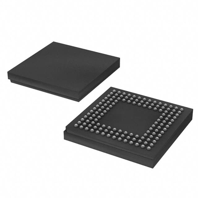
- Part No.:
- XC2C128-7CP132I
- Manufacturer:
- AMD
- Package:
- 132-TFBGA, CSPBGA
- Datasheet:
-
 XC2C128-7CP132I.pdf
- Description:
- IC CPLD 128MC 7NS 132CSPBGA
- Quantity:
- Payment:

- Shipping:

Inventory:3,309
Please send an inquiry. Send us your inquiry, and we will respond immediately.
Product details
Overview
XCKU035-1FBVA676C from AMD is a Kintex UltraScale FPGA device intended for configurable logic, embedded digital processing support, and interface concentration in embedded and communications systems. This orderable option combines the Kintex UltraScale architecture with 676-BBGA, FCBGA, which supports moderate-to-high FPGA I/O concentration with manageable board escape planning, allowing the design team to place board-specific logic, buffering, and connectivity functions into one FPGA platform rather than spreading them across multiple fixed-function devices.
Kintex UltraScale devices deliver high-end FPGA logic density, memory bandwidth support, and scalable connectivity for compute, communications, and acceleration hardware that need more headroom than 7-series platforms. For engineers reviewing the XCKU035-1FBVA676C datasheet, XCKU035-1FBVA676C pinout, XCKU035-1FBVA676C application, or XCKU035-1FBVA676C equivalent, this device is widely used in embedded processing platforms, digital interface bridges, industrial control systems, communications equipment, sensor aggregation hardware, and programmable accelerator subsystems.
Technical Context
In real hardware, XCKU035-1FBVA676C is used as an FPGA platform rather than a fixed-function controller. The selected Kintex UltraScale density and speed grade 1 orderable option. matter because logic capacity, memory blocks, DSP availability, and I/O reach all influence whether the device can absorb the intended control, buffering, and protocol workload.
The exact orderable code is important here: 676-BBGA, FCBGA affects escape routing and memory-interface planning, speed grade 1 orderable option. affects timing margin, and the commercial temperature option indicated by the suffix. determines whether the part can be approved for the target deployment range. That combination often decides which device is actually released into a production BOM.
Entry Kintex UltraScale density point for programmable logic platforms that need more integration and memory-side support than 7-series devices can comfortably provide. In practice, this means XCKU035-1FBVA676C is typically chosen when the system needs FPGA flexibility for control-heavy datapaths, local acceleration, interface bridging, or memory-connected logic while still respecting board-area and package constraints.
Key Specifications
| Parameter | Value and Actual Design Meaning |
|---|---|
| Device Type | Kintex UltraScale FPGA. |
| Series | Kintex UltraScale |
| Package | 676-BBGA, FCBGA package with tray packing. |
| Speed Grade | Speed grade 1 orderable option. |
| Operating Range | Commercial temperature option indicated by the suffix. |
| Architecture Role | Field-programmable logic device for configurable digital processing, interface adaptation, and subsystem integration. |
| Integration Focus | Used where programmable logic, memory connectivity, and board-specific digital control need to be consolidated. |
| Programming Model | Configuration-based FPGA platform within the referenced AMD family. |
Pinout & Package
The XCKU035-1FBVA676C pinout includes configurable user I/O, dedicated power rails, configuration and JTAG connections, clock-capable pins, and package-specific escape resources within 676-BBGA, FCBGA package.
For PCB design, the main concerns are clean power distribution, configuration-access planning, clock integrity, and package-aware escape routing around memory and high-activity interface banks.
| Pin / Function | PCB Design and Circuit Role |
|---|---|
| User I/O Pins | Configurable pins used for subsystem interfaces, memory buses, control signals, and application-specific logic connectivity. |
| Clock Inputs | Dedicated or clock-capable pins supporting timing distribution and synchronous FPGA operation. |
| Configuration / JTAG Pins | Used for device programming, configuration control, and boundary-scan access. |
| Power Rails | Support FPGA core, auxiliary, and I/O voltage domains required by the selected device family. |
| Ground Pins | Provide return paths for stable power integrity and high-speed digital operation. |
Key Features
- Configurable FPGA fabric supports board-specific logic, control, and interface integration.
- Package options scale I/O reach for compact through higher-density digital platforms.
- Orderable speed grades help align the device with board timing and interface targets.
- Suitable for consolidating subsystem logic, buffering, and programmable control functions.
- Supports embedded system flexibility across industrial, communications, and computing use cases.
- Field-programmable behavior preserves updateability across platform revisions.
Applications
| Embedded Processing Platforms | Industrial and Machine Control |
|---|---|
|
Use Scenario: Used in digital systems that need FPGA-based control, buffering, or local acceleration around processors and custom logic. IC Role: Provides configurable logic resources near embedded compute blocks. Use Value: Improves flexibility for evolving control and interface requirements. |
Use Scenario: Used in platforms that need programmable digital interfacing, timing coordination, and subsystem integration. IC Role: Acts as the configurable logic layer between sensors, memory, and control paths. Use Value: Supports maintainable and adaptable industrial hardware architectures. |
| Communications and Data Interfaces | Signal Aggregation and System Glue |
|
Use Scenario: Used where protocol bridging, framing logic, or board-level connectivity must stay field-programmable. IC Role: Implements adaptable interface engines and control-plane logic. Use Value: Helps avoid respins when interface requirements change. |
Use Scenario: Used to collect subsystem control, memory-side logic, and data-routing functions into one programmable device. IC Role: Centralizes digital support logic within the FPGA fabric. Use Value: Reduces auxiliary logic count while preserving scalability. |
Equivalent & Alternatives
When evaluating a XCKU035-1FBVA676C equivalent, engineers should compare family architecture, package, speed grade, operating range, memory-interface planning, and overall programmable logic fit.
| Alternative Part | Technical Difference | Application Difference | Selection Advice |
|---|---|---|---|
| XCKU035-1FBVA676C | Closely related orderable option in the same or adjacent family density with a different package, speed, or qualification emphasis. | Used when the board stays in the same general FPGA family but requires a different orderable fit. | Compare package, speed grade, temperature suffix, and validated system margins before substitution. |
| XCKU040-1FBVA676C | Alternative programmable logic option that can serve a similar subsystem role with a different density or family emphasis. | Used in comparable programmable-control or interface-heavy applications when the design tradeoff shifts. | Choose according to logic capacity, package routing, memory needs, and platform continuity. |
Compared with XCKU035-1FBVA676C, XCKU035-1FBVA676C selection depends on exact package, speed grade, qualification suffix, and board-routing fit. XCKU035-1FBVA676C vs XCKU040-1FBVA676C selection depends on whether the design should remain in the same FPGA family path or shift to another density or architecture with different integration tradeoffs.
Quality
XCKU035-1FBVA676C should be sourced as original AMD programmable logic inventory through traceable supply channels. Quality checks may include package inspection, top-mark validation, configuration access checks, and board-level bring-up verification.
Production validation should include power-sequencing review, configuration reliability, timing-closure confirmation, clock integrity checks, and signal-integrity review on high-activity I/O paths.
Availability
XCKU035-1FBVA676C is suitable for configurable digital logic, subsystem integration, and FPGA-based interface or control functions in embedded, industrial, and communications platforms.
Supply support may include volume procurement planning, scheduled delivery arrangements, traceable sourcing management, and long-term supply support for OEM, industrial electronics, automotive electronics, and embedded product programs. Sample and NPI supply support, as well as urgent in-stock supply support, can also be arranged for prototype builds, pilot runs, and time-critical production needs.
For production builds, confirming package option, speed grade, operating-range suffix, lifecycle status, and sourcing continuity helps reduce programmable-logic procurement risk.
Manufacturer
AMD is a semiconductor manufacturer whose adaptive computing and programmable logic portfolio includes FPGA devices, CPLDs, configuration solutions, embedded processing platforms, and related development technologies for industrial, communication, computing, automotive, and embedded electronic systems.
Kintex UltraScale devices deliver high-end FPGA logic density, memory bandwidth support, and scalable connectivity for compute, communications, and acceleration hardware that need more headroom than 7-series platforms. Entry Kintex UltraScale density point for programmable logic platforms that need more integration and memory-side support than 7-series devices can comfortably provide.
FAQ
What is XCKU035-1FBVA676C used for?
XCKU035-1FBVA676C is used for configurable logic, interface concentration, memory-side support, and embedded digital subsystem integration in FPGA-based hardware.
Where can I find the XCKU035-1FBVA676C datasheet download?
The XCKU035-1FBVA676C datasheet can be accessed from the confirmed source used for this FPGA family and orderable option.
What should be considered in XCKU035-1FBVA676C pinout design?
Designers should account for configuration access, power domains, clock planning, and package-driven escape routing around high-activity I/O and memory-related signals.
Is XCKU035-1FBVA676C a CPLD?
No. It is an FPGA orderable option in an AMD programmable logic family intended for broader configurable logic and subsystem integration tasks.
What are common XCKU035-1FBVA676C equivalent solutions?
Common candidates include XCKU035-1FBVA676C and XCKU040-1FBVA676C depending on package, family architecture, logic density, and system-level integration needs.
XC2C128-7CP132I Specifications
- Product attributes
- Attribute value
- Manufacturer:
- AMD
- Series:
- CoolRunner II
- Package/Case:
- 132-TFBGA, CSPBGA
- Packaging:
- Tray
- Product Status:
- Obsolete
- Programmable:
- Not Verified
- Programmable Type:
- In System Programmable
- Delay Time tpd(1) Max:
- 7 ns
- Voltage Supply - Internal:
- 1.7V ~ 1.9V
- Number of Logic Elements/Blocks:
- 8
- Number of Macrocells:
- 128
- Number of Gates:
- 3000
- Number of I/O:
- 100
- Operating Temperature:
- -40°C ~ 85°C (TA)
- Grade:
- -
- Qualification:
- -
- Mounting Type:
- Surface Mount
- Supplier Device Package:
- 132-CSPBGA (8x8)
XC2C128-7CP132I FAQ
1.How can I place an order for XC2C128-7CP132I through Aetrix?
Please submit a Request for Quotation (RFQ) for XC2C128-7CP132I on Aetrix. Our sales agent will provide a competitive quotation and guide you through the order confirmation once you accept the terms.
2.Are the price and stock information for XC2C128-7CP132I reliable?
The price and inventory of XC2C128-7CP132I are updated periodically and may fluctuate due to market conditions. Stock and pricing data are typically refreshed every 24 hours. Quotation validity for XC2C128-7CP132I is usually 5 days.
3.What payment methods are accepted for XC2C128-7CP132I?
We accept Wire Transfer, PayPal, Credit Card, Western Union, MoneyGram, and Escrow for XC2C128-7CP132I transactions.
Note: Certain payment methods may incur a processing fee.
4.How is shipping managed for XC2C128-7CP132I?
XC2C128-7CP132I orders can be shipped via leading logistics carriers, including DHL, UPS, FedEx, TNT, or Registered Mail.
Once your XC2C128-7CP132I order is processed, you will receive an email with the shipment details and tracking number.
Note: Tracking information may take up to 24 hours to appear. Express delivery typically takes 3–5 business days.
5.How can I obtain technical support or documentation for XC2C128-7CP132I?
For technical support, including XC2C128-7CP132I datasheets, pinout diagrams, or application guidance, please contact our engineering support team. They can provide detailed documentation and assistance for your XC2C128-7CP132I requirements.
6.How does Aetrix verify that XC2C128-7CP132I is sourced from the original manufacturer or authorized distributors?
All XC2C128-7CP132I products on Aetrix are procured from qualified distributors and authorized channels. Our dedicated quality assurance team conducts strict verification, including traceability checks and, if necessary, third-party testing. This ensures that XC2C128-7CP132I meets industry standards.
7.What is the process for return or replacement of XC2C128-7CP132I?
All XC2C128-7CP132I units undergo pre-shipment inspection (PSI). If there is an issue with XC2C128-7CP132I, returns or replacements are accepted under the following conditions:
1.Quantity discrepancies, incorrect items, or visible external defects (such as breakage or corrosion), acknowledged by Aetrix.
2.The issue is reported within 90 days of delivery.
3.The XC2C128-7CP132I part is unused and in its original packaging.
Return procedure for XC2C128-7CP132I:
1.Submit a request within 90 days.
2.Obtain a Return Material Authorization (RMA) from Aetrix.
XC2C128-7CP132I Tags
-
5M40ZE64C5N
Intel
-
ATF1502ASV-15AU44
Microchip Technology
-
5M80ZE64C5N
Intel
-
5M80ZT100C5N
Intel
-
ATF1502AS-10AU44
Microchip Technology
-
ATF1502AS-10JU44
Microchip Technology
-
5M80ZE64I5N
Intel
-
5M80ZT100I5N
Intel
-
LC4032V-75TN48C
Lattice Semiconductor Corporation
-
ATF1504ASV-15AU44
Microchip Technology
-
ATF1504AS-10JU44
Microchip Technology
-
5M160ZE64C5N
Intel
Tech Hub

Jumper cables guide covering safe connection order, red and black clamp placement, final ground connection, cable gauge, length, clamp quality, copper vs CCA cables, jump starter comparison and battery…

LDO regulator guide covering low dropout voltage, power dissipation, thermal design, PSRR, output noise, capacitor stability, adjustable LDO circuits, LDO vs buck converter and datasheet selection chec…

Conditional Access Module guide covering CAM meaning, CI/CI+ interface, smart card authorization, DVB security workflow, TV and set-top box compatibility, internal electronics, ESD protection, connecto…

Guide to electronic component obsolescence covering EOL risk, PCN/PDN notices, last-time buy planning, replacement options, form-fit-function validation, counterfeit risk and BOM lifecycle management.

18650 battery guide covering lithium-ion cell basics, 3.6V/3.7V voltage, 4.2V charging, mAh and Wh capacity, protected cells, chargers, BMS, series-parallel packs, holders, welding and sourcing checks.…

Hall effect sensor guide covering working principle, linear and digital sensors, Arduino circuits, current sensing, speed detection, automotive applications, A3144 examples, signal filtering and datash…

Product Change Notification guide for electronic components, covering PCN meaning, PCN vs PDN/EOL, common change types, risk levels, form-fit-function review, engineering validation, BOM control, LTB/L…

A practical guide to blend door actuators, covering HVAC function, symptoms, location, AC and heater issues, reset and calibration, replacement cost, electrical diagnosis, compatibility checks, and rep…

Engineering guide to Raspberry Pi alternatives, covering chip-level differences, Orange Pi, ROCK, Jetson, Banana Pi, NanoPi, Compute Module, Pico, GPIO, camera, HAT compatibility, and replacement risks…

Engineering guide to dynamic load response testing for high-current buck converters, covering load step setup, slew rate, Vcore undershoot, overshoot, recovery time, probe location, output capacitors a…


