
 My Inquiry
 My Account


AMD XC2VP2-6FG256C
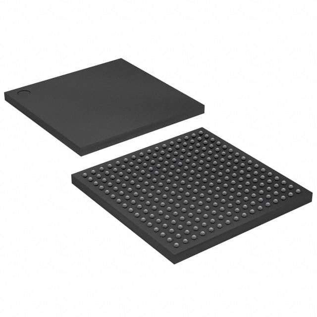
- Part No.:
- XC2VP2-6FG256C
- Manufacturer:
- AMD
- Category:
- FPGAs (Field Programmable Gate Array)
- Package:
- 256-BGA
- Datasheet:
-
 XC2VP2-6FG256C.pdf
- Description:
- IC FPGA 140 I/O 256FBGA
- Quantity:
- Payment:

- Shipping:

Inventory:3,541
Please send an inquiry. Send us your inquiry, and we will respond immediately.
Product details
Overview
XC2VP2-6FG256C from Xilinx is a Virtex-II Pro platform FPGA featuring 3,168 logic cells, 4 RocketIO multi-gigabit transceivers (2.5 Gb/s max), and no embedded PowerPC processor block. It uses a 0.13 µm copper process, 1.5 V core supply, and supports SelectIO-Ultra I/O standards including LVDS and PCI-X. It targets high-speed serial interconnect in telecom and networking equipment.
For engineers reviewing the XC2VP2-6FG256C datasheet, pinout, applications, or equivalent options, key selection factors include its FG256 wire-bond BGA package (256 balls, 1.0 mm pitch), -6 speed grade timing (DCM jitter, I/O setup/hold), RocketIO transceiver compliance with Fibre Channel and Gigabit Ethernet, and absence of PowerPC cores-making it suitable for pure programmable logic + SERDES applications without embedded processing.
Technical Context
The XC2VP2-6FG256C implements a SRAM-based FPGA architecture with Configurable Logic Blocks (CLBs), 18×18-bit dedicated multipliers, and 12 Block SelectRAM+ modules (18 Kb each). Its 4 RocketIO transceivers operate at up to 2.5 Gb/s in wire-bond packages and integrate monolithic clock recovery, 8B/10B encoding, and on-chip 50 Ω termination.
Digital Clock Manager (DCM) modules provide phase shifting, frequency synthesis, and deskew for internal clocks; IOBs support DDR/LVDS with Digitally Controlled Impedance (DCI); and routing uses Active Interconnect Technology with predictable delay independent of fanout.
Key Specifications
| Parameter | Value and Actual Design Meaning |
|---|---|
| Logic Cells | 3,168 - defines maximum combinational + sequential logic capacity for custom RTL implementation |
| RocketIO Transceivers | 4 × 2.5 Gb/s - enables four independent full-duplex serial links compliant with Fibre Channel and Gigabit Ethernet |
| Block RAM | 12 × 18 Kb SelectRAM+ - provides 216 KB of true dual-port embedded memory for FIFOs, buffers, or lookup tables |
| Multipliers | 44 × 18×18-bit - supports high-throughput DSP operations such as FIR filtering and FFT computation |
| I/O Pins | 140 user I/Os - supports high-pin-count parallel interfaces (e.g., DDR SDRAM, PCI-X) with programmable drive strength (2–24 mA) |
| Speed Grade | -6 - guarantees timing closure at 2.5 Gb/s transceiver operation and ≤350 MHz system clocking in commercial temperature range |
| Core Voltage | 1.5 V VCCINT - determines power delivery design, thermal management, and compatibility with standard 1.5 V regulator ICs |
Pinout & Package
XC2VP2-6FG256C is housed in a 256-ball Fine-Pitch Ball Grid Array (FG256) package with 1.0 mm pitch, wire-bond interconnect, and 140 user I/O pins. The package supports industrial-grade thermal dissipation and is Pb-free compatible (FGG256 variant available).
| Pin/Terminal | Circuit Role | Design Meaning |
|---|---|---|
| CCLK | Configuration Clock Input | Drives internal configuration shift register during master serial or SelectMAP programming |
| DONE | Configuration Status Output | Open-drain signal indicating successful bitstream loading and device initialization |
| M0–M2 | Mode Selection Inputs | Set configuration mode (e.g., slave serial, master SelectMAP) at power-up |
| PROG_B | Program Initiate Input | Active-low signal triggering full reconfiguration and clearing internal configuration memory |
| TCK/TMS/TDI/TDO | JTAG Boundary-Scan Interface | Enables IEEE 1149.1-compliant testing, debugging, and partial reconfiguration |
| DXP/DXN | RocketIO Differential Pair | One of four transceiver lanes supporting 2.5 Gb/s serial data with integrated CDR and 8B/10B encode/decode |
Key Features
| Feature | Design Value |
|---|---|
| RocketIO Transceivers | Four 2.5 Gb/s full-duplex SERDES channels with monolithic clock recovery eliminate need for external PLLs or retimers |
| SelectIO-Ultra I/O | Support for LVDS, PCI-X, SSTL, and HSTL standards with programmable drive strength (2–24 mA) and on-chip DCI termination simplifies board-level impedance matching |
| Digital Clock Manager (DCM) | Four DCMs enable precise clock deskew, integer/fractional frequency synthesis, and ±180° phase shifting for timing-critical interfaces like DDR or source-synchronous buses |
| Block SelectRAM+ | 12 × 18 Kb true dual-port RAM blocks allow concurrent read/write access per port-ideal for ping-pong buffering and real-time data streaming |
| 18×18 Multipliers | 44 hardwired multipliers deliver deterministic, low-latency arithmetic for DSP pipelines without consuming LUT resources |
Applications
| Telecom Line Card | Gigabit Ethernet Switch Fabric |
|---|---|
Use Scenario: Aggregating multiple T1/E1 or STM-1 streams into a backplane interface using time-division multiplexing. IC Role / Device Role / Timing Role: FPGA fabric implements HDLC framing, CRC generation, and channelized clock domain crossing; RocketIO handles serial backplane interconnect. Use Value: 2.5 Gb/s RocketIO links replace parallel bus traces, reducing PCB layer count and EMI while maintaining deterministic latency via DCM-controlled clock domains. | Use Scenario: Implementing a non-blocking 8-port Gigabit Ethernet switch with cut-through forwarding and VLAN tagging. IC Role / Device Role / Timing Role: XC2VP2-6FG256C serves as the packet switching engine, with RocketIO transceivers connecting to PHYs and CLBs executing MAC-layer logic and buffer management. Use Value: On-chip 18×18 multipliers accelerate CRC-32 computation; 140 I/Os support GMII/MII interfaces and external SRAM for packet buffering. |
| Fibre Channel Arbitrated Loop | High-Speed Test Equipment Interface |
Use Scenario: Building a Fibre Channel node controller for storage area network (SAN) edge devices operating at 1.0625 Gb/s. IC Role / Device Role / Timing Role: RocketIO transceivers implement FC-AL physical layer with 8B/10B encoding; CLBs run link-level state machines and buffer management logic. Use Value: Integrated 8B/10B encoder/decoder and on-chip 50 Ω termination reduce component count by eliminating external line drivers and serializer ICs. | Use Scenario: Serving as a high-bandwidth digital pattern generator in automated test equipment (ATE), driving multi-channel DUT interfaces at >200 MHz. IC Role / Device Role / Timing Role: FPGA fabric generates synchronized stimulus waveforms; RocketIO transceivers transmit calibration sequences over differential backplanes. Use Value: Four independent 2.5 Gb/s transceivers enable parallel test vector delivery across multiple DUT sites, improving throughput without increasing clock frequency. |
Equivalent & Alternatives
The following parts are listed as comparable options for similar FPGA + SERDES applications.
| Alternative Part | Technical Difference | Application Difference | Selection Advice |
|---|---|---|---|
| XC2VP4-6FG456C | 6,768 logic cells, 1 PowerPC 405 core, 4 RocketIO transceivers, 248 user I/Os, FG456 package | Includes embedded processor for control-plane offload; larger I/O count supports more parallel interfaces | Select when firmware-driven configuration, protocol stack execution, or higher logic density is required alongside SERDES |
| XC3S1000-4FG320C | No transceivers, 1,000,000 system gates, Spartan-3 architecture, 232 user I/Os, FG320 package | Pure logic-only device; lower cost but lacks high-speed serial I/O-requires external PHYs for Gigabit interfaces | Select for cost-sensitive, lower-bandwidth applications where serial transceivers are implemented externally or not needed |
Compared with XC2VP2-6FG256C, XC2VP4-6FG456C adds embedded processing capability and I/O headroom at higher cost and power, while XC3S1000-4FG320C sacrifices integrated SERDES for gate density and price-making XC2VP2-6FG256C optimal for fixed-function, transceiver-centric designs requiring minimal footprint and deterministic serial performance.
Availability
XC2VP2-6FG256C is available at Aetrix Electronics and suitable for telecom line cards, Gigabit Ethernet switch fabrics, Fibre Channel nodes, and high-speed test equipment requiring stable component supply and long-term obsolescence management.
Supply support for XC2VP2-6FG256C includes scheduled delivery planning, volume procurement assistance, BOM continuity management, traceable sourcing, and lifecycle availability coordination for OEM customers, industrial embedded developers, connected-device designers, and electronics production programs.
Manufacturer
Xilinx, Inc. is a semiconductor company specializing in programmable logic devices, acquired by AMD in 2022. It pioneered FPGA architectures with embedded hard IP and system-level integration.
The Virtex-II Pro family was designed for high-performance, mixed-signal system integration-combining FPGA fabric, multi-gigabit transceivers, and (in higher variants) PowerPC processors to replace ASICs in telecom, networking, and video infrastructure.
FAQ
What is the maximum data rate supported by the RocketIO transceivers in XC2VP2-6FG256C?
The XC2VP2-6FG256C supports RocketIO transceivers rated for up to 2.5 Gb/s in wire-bond packages like FG256. This rate complies with Fibre Channel (1.0625 Gb/s), Gigabit Ethernet (1.25 Gb/s), and 10G Attachment Unit Interface (XAUI) protocols. The -6 speed grade ensures timing closure at this rate under commercial temperature conditions. XC2VP2-6FG256C does not support RocketIO X (6.25 Gb/s), which is exclusive to Virtex-II Pro X devices.
Does XC2VP2-6FG256C include an embedded PowerPC processor core?
No, XC2VP2-6FG256C contains zero PowerPC 405 processor blocks. Per Table 1 in DS083, only XC2VP4 and higher Virtex-II Pro devices include one or two PowerPC cores. XC2VP2-6FG256C is optimized for pure programmable logic and serial transceiver applications without embedded software execution capability. This makes XC2VP2-6FG256C suitable for hardware-accelerated, real-time signal processing where deterministic latency is prioritized over firmware flexibility.
What package type and pin count does XC2VP2-6FG256C use?
XC2VP2-6FG256C uses the FG256 wire-bond fine-pitch BGA package with 256 balls arranged in a 1.0 mm pitch grid. It provides 140 user I/O pins, plus dedicated configuration, JTAG, and power/ground terminals. The FG256 package is distinct from flip-chip variants (e.g., FF672) and Pb-free FGG256 variants, all of which share identical pinout but differ in interconnect construction and RoHS compliance.
Can XC2VP2-6FG256C be configured via JTAG, and what modes are supported?
Yes, XC2VP2-6FG256C supports IEEE 1149.1 JTAG boundary-scan configuration through TCK, TMS, TDI, and TDO pins. It also supports slave-serial, master-serial, slave SelectMAP, master SelectMAP, and IEEE 1532 boundary-scan programming modes. JTAG enables in-system programming, debug access via ChipScope ILA, and readback of configuration memory and flip-flop states-critical for validation and field updates of XC2VP2-6FG256C-based systems.
What is the role of the Digital Clock Manager (DCM) in XC2VP2-6FG256C, and how many are available?
XC2VP2-6FG256C integrates four Digital Clock Manager (DCM) modules. Each DCM provides fully digital clock deskewing, frequency synthesis (integer/fractional multiplication/division), and fine-grained phase shifting (1/256 period resolution). These DCMs stabilize clock domains for source-synchronous interfaces like DDR SDRAM or RocketIO reference clocks, ensuring setup/hold timing margins. The presence of four DCMs allows independent clock domain management across multiple high-speed peripherals in XC2VP2-6FG256C designs.
XC2VP2-6FG256C Specifications
- Product attributes
- Attribute value
- Manufacturer:
- AMD
- Series:
- Virtex®-II Pro
- Package/Case:
- 256-BGA
- Packaging:
- Tray
- Product Status:
- Obsolete
- Programmable:
- Not Verified
- Number of LABs/CLBs:
- 352
- Number of Logic Elements/Cells:
- 3168
- Total RAM Bits:
- 221184
- Number of I/O:
- 140
- Number of Gates:
- -
- Voltage - Supply:
- 1.425V ~ 1.575V
- Mounting Type:
- Surface Mount
- Operating Temperature:
- 0°C ~ 85°C (TJ)
- Grade:
- -
- Qualification:
- -
- Supplier Device Package:
- 256-FBGA (17x17)
XC2VP2-6FG256C FAQ
1.How can I place an order for XC2VP2-6FG256C through Aetrix?
Please submit a Request for Quotation (RFQ) for XC2VP2-6FG256C on Aetrix. Our sales agent will provide a competitive quotation and guide you through the order confirmation once you accept the terms.
2.Are the price and stock information for XC2VP2-6FG256C reliable?
The price and inventory of XC2VP2-6FG256C are updated periodically and may fluctuate due to market conditions. Stock and pricing data are typically refreshed every 24 hours. Quotation validity for XC2VP2-6FG256C is usually 5 days.
3.What payment methods are accepted for XC2VP2-6FG256C?
We accept Wire Transfer, PayPal, Credit Card, Western Union, MoneyGram, and Escrow for XC2VP2-6FG256C transactions.
Note: Certain payment methods may incur a processing fee.
4.How is shipping managed for XC2VP2-6FG256C?
XC2VP2-6FG256C orders can be shipped via leading logistics carriers, including DHL, UPS, FedEx, TNT, or Registered Mail.
Once your XC2VP2-6FG256C order is processed, you will receive an email with the shipment details and tracking number.
Note: Tracking information may take up to 24 hours to appear. Express delivery typically takes 3–5 business days.
5.How can I obtain technical support or documentation for XC2VP2-6FG256C?
For technical support, including XC2VP2-6FG256C datasheets, pinout diagrams, or application guidance, please contact our engineering support team. They can provide detailed documentation and assistance for your XC2VP2-6FG256C requirements.
6.How does Aetrix verify that XC2VP2-6FG256C is sourced from the original manufacturer or authorized distributors?
All XC2VP2-6FG256C products on Aetrix are procured from qualified distributors and authorized channels. Our dedicated quality assurance team conducts strict verification, including traceability checks and, if necessary, third-party testing. This ensures that XC2VP2-6FG256C meets industry standards.
7.What is the process for return or replacement of XC2VP2-6FG256C?
All XC2VP2-6FG256C units undergo pre-shipment inspection (PSI). If there is an issue with XC2VP2-6FG256C, returns or replacements are accepted under the following conditions:
1.Quantity discrepancies, incorrect items, or visible external defects (such as breakage or corrosion), acknowledged by Aetrix.
2.The issue is reported within 90 days of delivery.
3.The XC2VP2-6FG256C part is unused and in its original packaging.
Return procedure for XC2VP2-6FG256C:
1.Submit a request within 90 days.
2.Obtain a Return Material Authorization (RMA) from Aetrix.
XC2VP2-6FG256C Tags
-
ICE40LP384-SG32
Lattice Semiconductor Corporation
-
ICE40UL640-CM36AI
Lattice Semiconductor Corporation
-
ICE40UL1K-CM36AI
Lattice Semiconductor Corporation
-
LCMXO2-256HC-4SG32C
Lattice Semiconductor Corporation
-
10M02DCV36C8G
Intel
-
LCMXO2-256HC-4SG32I
Lattice Semiconductor Corporation
-
ICE5LP1K-SG48ITR
Lattice Semiconductor Corporation
-
ICE40LP1K-CM36
Lattice Semiconductor Corporation
-
LCMXO2-256ZE-1SG32I
Lattice Semiconductor Corporation
-
LCMXO2-256HC-4SG48I
Lattice Semiconductor Corporation
-
ICE40LP1K-CM81
Lattice Semiconductor Corporation

-
T20W80I4
Efinix, Inc.
Tech Hub

A practical engineering and sourcing framework covering lifecycle verification, lifetime-buy calculations, replacement qualification, supplier checks and counterfeit-risk controls.

TTL and CMOS logic families differ in thresholds, loading, output drive, power and timing. This engineering guide compares 74HC and 74HCT, calculates noise margins and checks 3.3 V/5 V compatibility.

A practical engineering guide to 3.3V and 5V logic compatibility, input thresholds, resistor dividers, translator ICs, MOSFET level shifting, I2C pull-ups, timing limits and power-sequencing risks.

The 74HC595 uses push-pull logic outputs, while the TPIC6B595 uses 50 V open-drain DMOS sinks for higher-power loads. This guide compares timing, current limits, 3.3 V interfacing, load wiring, thermal…

The 74HC595 converts serial data into eight stable parallel outputs. This guide covers pin functions, shift and storage timing, OE and MR behavior, drive-current limits, cascading, voltage compatibilit…

A technical comparison of level-sensitive latches and edge-triggered flip-flops, covering timing windows, setup and hold limits, master–slave operation, time borrowing, race-through, HDL inference and…

A D latch stores one bit while Enable controls when data can pass. This reference covers gate-level operation, truth tables, transparency, setup and hold timing, LE versus OE, common ICs and practical …

An SR latch stores one bit through cross-coupled feedback. This engineering reference covers NOR and NAND implementations, truth tables, forbidden-state recovery, gated operation, switch debouncing, fa…

Latch circuits retain one bit through feedback. This technical reference covers SR and D latches, truth tables, transparency, timing limits, latch-versus-flip-flop behavior, applications and common log…

An engineering guide to LED driver operation, constant-current and constant-voltage outputs, linear and switching topologies, dimming, IC selection, calculations, replacement compatibility, and fault c…


