
 My Inquiry
 My Account


AMD XC4005E-1PQ208C
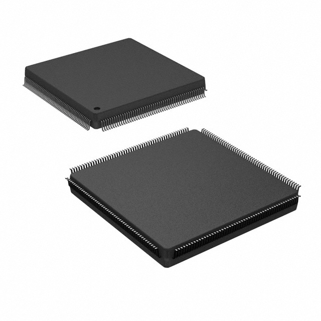
- Part No.:
- XC4005E-1PQ208C
- Manufacturer:
- AMD
- Category:
- FPGAs (Field Programmable Gate Array)
- Package:
- 208-BFQFP
- Datasheet:
-
 XC4005E-1PQ208C.pdf
- Description:
- IC FPGA 112 I/O 208QFP
- Quantity:
- Payment:

- Shipping:

Inventory:3,431
Please send an inquiry. Send us your inquiry, and we will respond immediately.
Product details
Overview
XC4005E-1PQ208C from Xilinx is a Field-Programmable Gate Array (FPGA) with 5,000 usable gates, 208-pin Plastic Quad Flat Package (PQFP), -1 speed grade (10 ns CLB propagation delay), and commercial temperature range (0°C to 70°C). It implements synchronous digital logic in embedded control, protocol bridging, and glue-logic replacement applications.
For engineers reviewing the XC4005E-1PQ208C datasheet, pinout, applications, or equivalent options, key selection criteria include gate count, I/O count (168 user I/Os), speed grade (-1), package thermal profile, and compatibility with Xilinx Foundation Series design tools.
Technical Context
The XC4005E-1PQ208C belongs to the Xilinx XC4000E family, built on 0.5 µm CMOS technology with configurable logic blocks (CLBs), input/output blocks (IOBs), and interconnect resources. It supports SRAM-based configuration via JTAG or serial PROM and includes dedicated carry logic for arithmetic functions.
It features programmable I/O standards including LVTTL and TTL-compatible inputs, internal 3.3 V or 5 V VCCINT operation, and configurable slew rate and drive strength per IOB. Configuration memory is volatile and requires external initialization at power-up.
Key Specifications
| Parameter | Value and Actual Design Meaning |
|---|---|
| Gates | 5,000 usable system gates - determines maximum combinational logic density for logic synthesis |
| Speed Grade | -1 (10 ns CLB tPD) - specifies worst-case propagation delay through a CLB for timing closure |
| Package | PQ208 - 208-pin plastic quad flat pack with 0.5 mm pitch; requires standard QFP reflow profile |
| User I/Os | 168 - number of bidirectional, configurable pins available for system interface and signal routing |
| Operating Temp | 0°C to 70°C - defines ambient temperature range for guaranteed electrical performance |
| VCCINT | 5.0 V ± 5% - core supply voltage required for internal logic array operation |
Pinout & Package
PQ208 is a 28 × 28 mm plastic quad flat package with gull-wing leads, JEDEC MS-026 compliant, suitable for surface-mount assembly and standard PCB trace routing.
| Pin/Terminal | Circuit Role | Design Meaning |
|---|---|---|
| GND | Ground reference | Multiple dedicated pins provide low-impedance return path for core and I/O circuits |
| VCCINT | Core power supply | 5 V supply for internal CLB and interconnect logic; decoupling required per Xilinx layout guidelines |
| VCCO | I/O power supply | Configurable per bank (3.3 V or 5 V); sets output voltage level and input threshold for associated I/Os |
| PROGRAM | Configuration reset | Active-low signal that clears configuration memory and initiates reload from external source |
| DIN | Serial configuration data input | Accepts bitstream during master serial mode; connects to PROM or microcontroller |
| TCK/TMS/TDI/TDO | JTAG boundary-scan interface | IEEE 1149.1-compliant test and programming interface; enables in-system configuration and debug |
Key Features
| Feature | Design Value |
|---|---|
| Configurable CLBs | Each CLB contains two 3-input LUTs and flip-flops, enabling flexible synchronous logic implementation |
| Dedicated carry chain | Fast ripple-carry path across CLBs for efficient counter and arithmetic block synthesis |
| Per-bank I/O voltage control | Allows mixed-voltage interfacing (e.g., 5 V CPU with 3.3 V peripheral) without level shifters |
| Four-quadrant interconnect | Provides predictable routing delay and high fan-out capability across the device fabric |
| JTAG boundary scan | Supports IEEE 1149.1 compliance for board-level test, configuration, and debugging |
Applications
| Industrial PLC Logic Controller | Legacy Bus Interface Bridge |
|---|---|
Use Scenario: Replacing discrete TTL logic in programmable logic controller backplanes requiring field-upgradable control sequences. IC Role / Device Role / Timing Role: Glue logic replacement and state-machine executor with deterministic 10 ns CLB timing. Use Value: Reduces board space by consolidating >50 SSI/MSI ICs into single XC4005E-1PQ208C while supporting firmware updates via JTAG. | Use Scenario: Translating between ISA bus timing and modern microcontroller peripherals in retro-computing hardware upgrades. IC Role / Device Role / Timing Role: Protocol translator with programmable setup/hold timing and strobe generation. Use Value: Enables precise cycle-accurate ISA signal alignment using XC4005E-1PQ208C's dedicated carry chain and registered I/O paths. |
| Automotive Diagnostic Tool Interface | Test Equipment Pattern Generator |
Use Scenario: Implementing ISO 9141-2 and K-Line physical layer handshaking in handheld OBD-II diagnostic adapters. IC Role / Device Role / Timing Role: Digital timing controller managing baud-rate-dependent edge placement and response latency. Use Value: Achieves sub-microsecond timing resolution using XC4005E-1PQ208C's 10 ns CLB delay and programmable I/O slew rates. | Use Scenario: Generating synchronized multi-channel digital stimulus waveforms for IC functional validation. IC Role / Device Role / Timing Role: Deterministic pattern sequencer with parallel output and clock-domain crossing support. Use Value: Delivers repeatable 10 ns timing edges across 168 I/Os using XC4005E-1PQ208C's global clock network and registered outputs. |
Equivalent & Alternatives
The following parts are listed as comparable options for similar FPGA logic implementation applications.
| Alternative Part | Technical Difference | Application Difference | Selection Advice |
|---|---|---|---|
| XC4005E-2PQ208C | Slower -2 speed grade (12 ns CLB tPD); otherwise identical architecture and pinout | Suitable where timing margin allows relaxed setup/hold constraints | Select when lower power or cost priority outweighs maximum operating frequency |
| XCS10-PC84C | Smaller 10,000-gate capacity, 84-pin PLCC package, no dedicated carry chain | Limited to simpler control logic; incompatible pinout and routing resources | Choose only for space-constrained legacy PLCC designs with minimal logic depth |
Compared with XC4005E-1PQ208C, the -2 variant trades 2 ns timing margin for potential cost reduction, while XCS10-PC84C offers higher gate count but lacks carry logic and requires PCB redesign due to different package and I/O structure.
Availability
XC4005E-1PQ208C is available at Aetrix Electronics and suitable for industrial control, legacy system refurbishment, and test equipment design requiring stable component supply and long-term obsolescence management.
Supply support for XC4005E-1PQ208C includes scheduled delivery planning, volume procurement assistance, BOM continuity management, traceable sourcing, and lifecycle availability coordination for OEM customers, industrial embedded developers, connected-device designers, and electronics production programs.
Manufacturer
Xilinx, now part of AMD, pioneered commercial FPGA technology and developed scalable programmable logic architectures for system-level integration.
The XC4000E family was designed for cost-sensitive, medium-complexity digital logic replacement in industrial, automotive, and communications equipment with emphasis on ease of design reuse and JTAG configurability.
FAQ
What is the maximum operating frequency supported by XC4005E-1PQ208C?
The XC4005E-1PQ208C has a -1 speed grade specifying 10 ns CLB propagation delay. Maximum system clock frequency depends on design topology, but typical register-to-register paths achieve 80–100 MHz in well-optimized implementations. The actual achievable frequency must be verified using Xilinx PAR and timing analyzer tools on the specific placed-and-routed netlist for XC4005E-1PQ208C.
Does XC4005E-1PQ208C support in-system programming?
Yes, XC4005E-1PQ208C supports in-system programming via its IEEE 1149.1 JTAG interface (TCK/TMS/TDI/TDO pins). Configuration bitstream can be loaded dynamically using boundary-scan controllers or Xilinx programming cables. The device does not retain configuration after power loss, so external PROM or host processor initialization is required at boot for XC4005E-1PQ208C.
What power supply voltages are required for XC4005E-1PQ208C operation?
XC4005E-1PQ208C requires two separate supplies: VCCINT = 5.0 V ± 5% for the core logic array, and VCCO = 5.0 V (or 3.3 V if configured for LVTTL) for I/O banks. Each supply must be independently decoupled with low-ESR capacitors close to respective power pins as specified in the XC4005E-1PQ208C Hardware User Guide.
Is XC4005E-1PQ208C pin-compatible with other XC4000E family members in PQ208 package?
Yes, all XC4000E devices in the PQ208 package-including XC4005E-1PQ208C, XC4010E-1PQ208C, and XC4015E-1PQ208C-share identical pinouts and I/O banking structure. This allows direct substitution within the same footprint when gate count and speed grade requirements align, provided configuration bitstream is regenerated for the target device size.
What software tools are required to develop for XC4005E-1PQ208C?
Xilinx Foundation Series 2.x or later (including WebPACK ISE versions supporting XC4000E) is required for synthesis, mapping, place-and-route, and bitstream generation for XC4005E-1PQ208C. Programming is performed using Xilinx IMPACT or third-party JTAG tools compatible with IEEE 1149.1. Legacy schematic entry and ABEL support is also available for XC4005E-1PQ208C design flow.
XC4005E-1PQ208C Specifications
- Product attributes
- Attribute value
- Manufacturer:
- AMD
- Series:
- XC4000E/X
- Package/Case:
- 208-BFQFP
- Packaging:
- Tray
- Product Status:
- Obsolete
- Programmable:
- Not Verified
- Number of LABs/CLBs:
- 196
- Number of Logic Elements/Cells:
- 466
- Total RAM Bits:
- 6272
- Number of I/O:
- 112
- Number of Gates:
- 5000
- Voltage - Supply:
- 4.75V ~ 5.25V
- Mounting Type:
- Surface Mount
- Operating Temperature:
- 0°C ~ 85°C (TJ)
- Grade:
- -
- Qualification:
- -
- Supplier Device Package:
- 208-PQFP (28x28)
XC4005E-1PQ208C FAQ
1.How can I place an order for XC4005E-1PQ208C through Aetrix?
Please submit a Request for Quotation (RFQ) for XC4005E-1PQ208C on Aetrix. Our sales agent will provide a competitive quotation and guide you through the order confirmation once you accept the terms.
2.Are the price and stock information for XC4005E-1PQ208C reliable?
The price and inventory of XC4005E-1PQ208C are updated periodically and may fluctuate due to market conditions. Stock and pricing data are typically refreshed every 24 hours. Quotation validity for XC4005E-1PQ208C is usually 5 days.
3.What payment methods are accepted for XC4005E-1PQ208C?
We accept Wire Transfer, PayPal, Credit Card, Western Union, MoneyGram, and Escrow for XC4005E-1PQ208C transactions.
Note: Certain payment methods may incur a processing fee.
4.How is shipping managed for XC4005E-1PQ208C?
XC4005E-1PQ208C orders can be shipped via leading logistics carriers, including DHL, UPS, FedEx, TNT, or Registered Mail.
Once your XC4005E-1PQ208C order is processed, you will receive an email with the shipment details and tracking number.
Note: Tracking information may take up to 24 hours to appear. Express delivery typically takes 3–5 business days.
5.How can I obtain technical support or documentation for XC4005E-1PQ208C?
For technical support, including XC4005E-1PQ208C datasheets, pinout diagrams, or application guidance, please contact our engineering support team. They can provide detailed documentation and assistance for your XC4005E-1PQ208C requirements.
6.How does Aetrix verify that XC4005E-1PQ208C is sourced from the original manufacturer or authorized distributors?
All XC4005E-1PQ208C products on Aetrix are procured from qualified distributors and authorized channels. Our dedicated quality assurance team conducts strict verification, including traceability checks and, if necessary, third-party testing. This ensures that XC4005E-1PQ208C meets industry standards.
7.What is the process for return or replacement of XC4005E-1PQ208C?
All XC4005E-1PQ208C units undergo pre-shipment inspection (PSI). If there is an issue with XC4005E-1PQ208C, returns or replacements are accepted under the following conditions:
1.Quantity discrepancies, incorrect items, or visible external defects (such as breakage or corrosion), acknowledged by Aetrix.
2.The issue is reported within 90 days of delivery.
3.The XC4005E-1PQ208C part is unused and in its original packaging.
Return procedure for XC4005E-1PQ208C:
1.Submit a request within 90 days.
2.Obtain a Return Material Authorization (RMA) from Aetrix.
XC4005E-1PQ208C Tags
-
ICE40LP384-SG32
Lattice Semiconductor Corporation
-
ICE40UL640-CM36AI
Lattice Semiconductor Corporation
-
ICE40UL1K-CM36AI
Lattice Semiconductor Corporation
-
LCMXO2-256HC-4SG32C
Lattice Semiconductor Corporation
-
10M02DCV36C8G
Intel
-
LCMXO2-256HC-4SG32I
Lattice Semiconductor Corporation
-
ICE5LP1K-SG48ITR
Lattice Semiconductor Corporation
-
ICE40LP1K-CM36
Lattice Semiconductor Corporation
-
LCMXO2-256ZE-1SG32I
Lattice Semiconductor Corporation
-
LCMXO2-256HC-4SG48I
Lattice Semiconductor Corporation
-
ICE40LP1K-CM81
Lattice Semiconductor Corporation

-
T20W80I4
Efinix, Inc.
Tech Hub

A practical engineering and sourcing framework covering lifecycle verification, lifetime-buy calculations, replacement qualification, supplier checks and counterfeit-risk controls.

TTL and CMOS logic families differ in thresholds, loading, output drive, power and timing. This engineering guide compares 74HC and 74HCT, calculates noise margins and checks 3.3 V/5 V compatibility.

A practical engineering guide to 3.3V and 5V logic compatibility, input thresholds, resistor dividers, translator ICs, MOSFET level shifting, I2C pull-ups, timing limits and power-sequencing risks.

The 74HC595 uses push-pull logic outputs, while the TPIC6B595 uses 50 V open-drain DMOS sinks for higher-power loads. This guide compares timing, current limits, 3.3 V interfacing, load wiring, thermal…

The 74HC595 converts serial data into eight stable parallel outputs. This guide covers pin functions, shift and storage timing, OE and MR behavior, drive-current limits, cascading, voltage compatibilit…

A technical comparison of level-sensitive latches and edge-triggered flip-flops, covering timing windows, setup and hold limits, master–slave operation, time borrowing, race-through, HDL inference and…

A D latch stores one bit while Enable controls when data can pass. This reference covers gate-level operation, truth tables, transparency, setup and hold timing, LE versus OE, common ICs and practical …

An SR latch stores one bit through cross-coupled feedback. This engineering reference covers NOR and NAND implementations, truth tables, forbidden-state recovery, gated operation, switch debouncing, fa…

Latch circuits retain one bit through feedback. This technical reference covers SR and D latches, truth tables, transparency, timing limits, latch-versus-flip-flop behavior, applications and common log…

An engineering guide to LED driver operation, constant-current and constant-voltage outputs, linear and switching topologies, dimming, IC selection, calculations, replacement compatibility, and fault c…


