
 My Inquiry
 My Account


AMD XC7VX485T-2FFG1157C
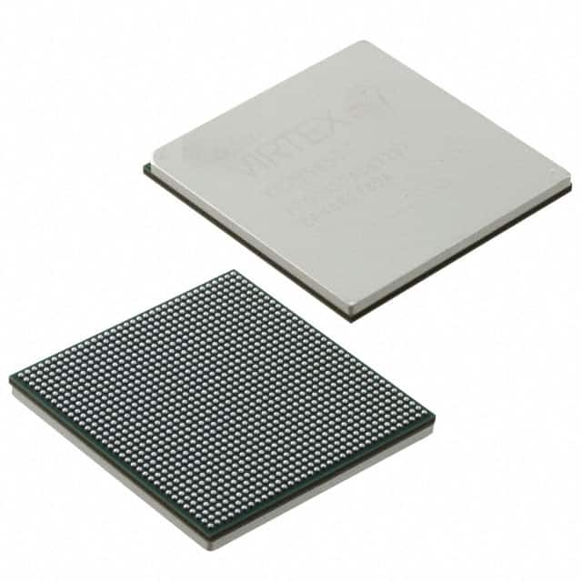
- Part No.:
- XC7VX485T-2FFG1157C
- Manufacturer:
- AMD
- Category:
- FPGAs (Field Programmable Gate Array)
- Package:
- 1156-BBGA, FCBGA
- Datasheet:
-
 XC7VX485T-2FFG1157C.pdf
- Description:
- IC FPGA 600 I/O 1157FCBGA
- Quantity:
- Payment:

- Shipping:

Inventory:1,469
Please send an inquiry. Send us your inquiry, and we will respond immediately.
Product details
Overview
XC7VX485T-2FFG1157C from AMD is a high-performance 28 nm Virtex-7 FPGA with 485,760 logic cells, 2,825 DSP slices, and 34.8 Mb of block RAM. It features 700 GT transceivers operating up to 13.1 Gb/s, supports PCIe Gen3 x8, and is used in high-speed data acquisition and radar signal processing systems.
For engineers reviewing the XC7VX485T-2FFG1157C datasheet, pinout, applications, or equivalent options, key selection factors include transceiver lane count and speed, I/O bank voltage flexibility (1.2 V to 1.8 V), thermal performance in air-cooled 1157-pin FCBGA packages, and support for JTAG and SelectMAP configuration interfaces.
Technical Context
The XC7VX485T-2FFG1157C implements a 28 nm HKMG process-based architecture with configurable logic blocks (CLBs), 36 Kb block RAMs, and hardened IP including PCIe Gen3 endpoints, 10/100/1000 Ethernet MACs, and AXI interconnects. It supports multi-voltage I/O banks (1.2 V, 1.35 V, 1.5 V, 1.8 V) and offers programmable delay and slew rate control per I/O.
Configuration is supported via Master SPI, Slave SelectMAP, or JTAG modes, with bitstream encryption using AES-256 and HMAC authentication. The device includes internal analog monitoring for on-chip temperature and supply voltage, accessible through XADC interface channels.
Key Specifications
| Parameter | Value and Actual Design Meaning |
|---|---|
| Logic Cells | 485,760 - total available LUT-based fabric resources for custom digital logic implementation |
| DSP Slices | 2,825 - dedicated arithmetic units supporting 25×18 signed multiply-accumulate operations per slice |
| Block RAM | 34.8 Mb - configurable memory blocks usable as true dual-port RAM, FIFO, or ROM |
| GT Transceivers | 700 lanes - high-speed serial I/O supporting protocols including PCIe Gen3, SRIO, and CPRI |
| Max GT Rate | 13.1 Gb/s - sustained line rate per transceiver lane under specified thermal and signal integrity conditions |
| I/O Pins | 500 - user-configurable single-ended or differential I/O across 24 selectable voltage banks |
| Configuration Interface | JTAG/SelectMAP/SPI - enables in-system programming, boundary-scan testing, and parallel loading |
Pinout & Package
The XC7VX485T-2FFG1157C is housed in a 1157-pin Flip-Chip Ball Grid Array (FCBGA) package with 35 mm × 35 mm body size, 1.0 mm ball pitch, and thermal lid for enhanced heat dissipation in high-power operation.
| Pin/Terminal | Circuit Role | Design Meaning |
|---|---|---|
| M0–M2 | Mode Configuration | Selects boot mode (JTAG, SPI, SelectMAP) at power-up |
| CCLK | Configuration Clock | Drives clock input for Master SPI configuration; bidirectional in SelectMAP mode |
| DIN / DOUT | Serial Data I/O | Input for SPI configuration; output for readback or status reporting |
| INIT_B | Configuration Status | Open-drain active-low signal indicating configuration memory readiness or error |
| PROGRAM_B | Configuration Reset | Active-low asynchronous reset that clears configuration memory and restarts boot sequence |
| CLK_0–CLK_3 | Global Clock Inputs | Dedicated low-skew inputs feeding MMCM/PLL clock management resources |
Key Features
| Feature | Design Value |
|---|---|
| Hardened PCIe Gen3 Endpoint | Integrated root port and endpoint logic supporting x1/x2/x4/x8 link widths without external PHY |
| AES-256 Bitstream Encryption | Prevents unauthorized access or cloning by encrypting configuration bitstream stored in external flash |
| XADC Monitoring | On-die 12-bit ADC with dual analog inputs for real-time die temperature and supply voltage measurement |
| Multi-Voltage I/O Banks | 24 independent banks supporting simultaneous 1.2 V, 1.35 V, 1.5 V, and 1.8 V signaling standards |
| Transceiver Clocking | Dedicated reference clock inputs per GT group with internal PLL/MMCM for jitter reduction and frequency synthesis |
Applications
| Radar Signal Processing | High-Speed Test Equipment |
|---|---|
Use Scenario: Real-time beamforming and pulse-Doppler processing in phased-array radar systems requiring deterministic latency and high throughput. IC Role / Device Role / Timing Role: Primary compute fabric handling FFT, CFAR, and digital down-conversion with synchronized GT transceivers feeding ADC/DAC interfaces. Use Value: 700 GT lanes at 13.1 Gb/s enable direct connection to high-resolution RF sampling ADCs (e.g., AD9680), eliminating intermediate serialization stages. | Use Scenario: Automated test equipment for semiconductor validation requiring pattern generation, response capture, and protocol analysis at multi-Gbps rates. IC Role / Device Role / Timing Role: Reconfigurable protocol engine implementing custom JESD204B, MIPI D-PHY, or SATA physical layers with precise timing control. Use Value: 2,825 DSP slices allow concurrent execution of real-time error detection, BER calculation, and waveform synthesis algorithms. |
| Medical Imaging Backend | Low-Latency Financial Trading |
Use Scenario: CT and MRI image reconstruction pipelines where raw sensor data must be processed and streamed to GPU-accelerated visualization subsystems. IC Role / Device Role / Timing Role: High-bandwidth bridging device aggregating multiple 10 GbE or Aurora links into coherent AXI4-Stream data flows for downstream compute. Use Value: 34.8 Mb of block RAM provides deep buffering for multi-frame DICOM packet assembly without external memory latency. | Use Scenario: Ultra-low-latency market data feed handlers and order routing engines deployed in co-located data centers. IC Role / Device Role / Timing Role: Deterministic packet parser and classifier accelerating FIX/OUCH protocol decoding with sub-100 ns pipeline latency. Use Value: 485,760 logic cells support fully pipelined, parallel state machines that sustain >10 Mmsg/s throughput at <50 ns jitter. |
Equivalent & Alternatives
The following parts are listed as comparable options for similar high-end FPGA applications.
| Alternative Part | Technical Difference | Application Difference | Selection Advice |
|---|---|---|---|
| XCVU13P-2FLGA2577E | UltraScale+ architecture; higher logic density (1,024K LC), lower GT count (528), 16.3 Gb/s max GT rate | Better suited for AI inference acceleration and 100G Ethernet switching; less optimal for wide-lane radar I/O aggregation | Select when migrating to 16 nm node for improved power efficiency and embedded DDR4 controller integration |
| XC7VX690T-2FFG1927I | Larger package (1927-pin), +43% logic cells (693,120), same 28 nm process and GT spec (13.1 Gb/s) | Used in full-scale software-defined radio baseband processing where additional CLBs support multi-standard modulation stacks | Choose for designs requiring maximum fabric headroom within Virtex-7 family and compatible toolchain flow |
Compared with XC7VX485T-2FFG1157C, the XCVU13P-2FLGA2577E delivers higher per-watt compute but requires board redesign due to different package and power delivery; the XC7VX690T-2FFG1927I offers seamless migration path with identical I/O electrical behavior and timing models.
Availability
XC7VX485T-2FFG1157C is available at Aetrix Electronics and suitable for radar signal processing, high-speed test instrumentation, and medical imaging backend systems requiring stable component supply over extended production lifecycles.
Supply support for XC7VX485T-2FFG1157C includes scheduled delivery planning, volume procurement assistance, BOM continuity management, traceable sourcing, and lifecycle availability coordination for OEM customers, industrial embedded developers, connected-device designers, and electronics production programs.
Manufacturer
AMD is a global semiconductor company designing adaptive computing platforms for data center, AI, embedded, and aerospace applications.
The Virtex-7 family targets high-throughput, low-latency system-level integration in defense electronics, scientific instrumentation, and next-generation communications infrastructure.
FAQ
What is the maximum supported transceiver data rate for XC7VX485T-2FFG1157C?
The XC7VX485T-2FFG1157C supports a maximum transceiver line rate of 13.1 Gb/s per GT lane under standard operating conditions (junction temperature ≤ 100°C, proper reference clock jitter profile). This rate is validated for protocols including PCIe Gen3 and CPRI. The XC7VX485T-2FFG1157C achieves this using its dedicated GT reference clock inputs and internal QPLL/CPLL clocking architecture.
Does XC7VX485T-2FFG1157C include built-in security features for bitstream protection?
Yes, the XC7VX485T-2FFG1157C integrates AES-256 encryption and HMAC authentication for secure bitstream loading. These features prevent unauthorized readback or cloning of the configuration. The XC7VX485T-2FFG1157C uses on-chip key storage and supports both volatile and non-volatile key programming methods defined in UG470.
What configuration modes are supported by XC7VX485T-2FFG1157C?
The XC7VX485T-2FFG1157C supports three primary configuration modes: Master SPI (using on-chip oscillator), Slave SelectMAP (parallel synchronous loading), and JTAG (boundary-scan and debug). Mode selection is controlled by M0–M2 pins at power-up. The XC7VX485T-2FFG1157C also supports fallback configuration and multi-boot via external flash partitioning.
Can XC7VX485T-2FFG1157C operate with mixed I/O voltage standards on the same device?
Yes, the XC7VX485T-2FFG1157C supports simultaneous operation of multiple I/O standards across its 24 independent banks, each configurable for 1.2 V, 1.35 V, 1.5 V, or 1.8 V. This allows direct interfacing with diverse peripherals such as DDR3L memory, CMOS sensors, and legacy LVDS devices without level-shifting. The XC7VX485T-2FFG1157C enforces strict bank-wise voltage compliance per UG475.
What thermal management considerations apply to XC7VX485T-2FFG1157C in continuous operation?
The XC7VX485T-2FFG1157C requires active airflow or heatsink mounting due to its 25–35 W typical power dissipation range. Its FCBGA package includes a thermal lid optimized for conduction cooling. Thermal design must maintain junction temperature below 100°C per UG475; the XC7VX485T-2FFG1157C provides on-die temperature sensing via XADC for closed-loop thermal monitoring.
XC7VX485T-2FFG1157C Specifications
- Product attributes
- Attribute value
- Manufacturer:
- AMD
- Series:
- Virtex®-7 XT
- Package/Case:
- 1156-BBGA, FCBGA
- Packaging:
- Tray
- Product Status:
- Active
- Programmable:
- Not Verified
- Number of LABs/CLBs:
- 37950
- Number of Logic Elements/Cells:
- 485760
- Total RAM Bits:
- 37969920
- Number of I/O:
- 600
- Number of Gates:
- -
- Voltage - Supply:
- 0.97V ~ 1.03V
- Mounting Type:
- Surface Mount
- Operating Temperature:
- 0°C ~ 85°C (TJ)
- Grade:
- -
- Qualification:
- -
- Supplier Device Package:
- 1157-FCBGA (35x35)
XC7VX485T-2FFG1157C FAQ
1.How can I place an order for XC7VX485T-2FFG1157C through Aetrix?
Please submit a Request for Quotation (RFQ) for XC7VX485T-2FFG1157C on Aetrix. Our sales agent will provide a competitive quotation and guide you through the order confirmation once you accept the terms.
2.Are the price and stock information for XC7VX485T-2FFG1157C reliable?
The price and inventory of XC7VX485T-2FFG1157C are updated periodically and may fluctuate due to market conditions. Stock and pricing data are typically refreshed every 24 hours. Quotation validity for XC7VX485T-2FFG1157C is usually 5 days.
3.What payment methods are accepted for XC7VX485T-2FFG1157C?
We accept Wire Transfer, PayPal, Credit Card, Western Union, MoneyGram, and Escrow for XC7VX485T-2FFG1157C transactions.
Note: Certain payment methods may incur a processing fee.
4.How is shipping managed for XC7VX485T-2FFG1157C?
XC7VX485T-2FFG1157C orders can be shipped via leading logistics carriers, including DHL, UPS, FedEx, TNT, or Registered Mail.
Once your XC7VX485T-2FFG1157C order is processed, you will receive an email with the shipment details and tracking number.
Note: Tracking information may take up to 24 hours to appear. Express delivery typically takes 3–5 business days.
5.How can I obtain technical support or documentation for XC7VX485T-2FFG1157C?
For technical support, including XC7VX485T-2FFG1157C datasheets, pinout diagrams, or application guidance, please contact our engineering support team. They can provide detailed documentation and assistance for your XC7VX485T-2FFG1157C requirements.
6.How does Aetrix verify that XC7VX485T-2FFG1157C is sourced from the original manufacturer or authorized distributors?
All XC7VX485T-2FFG1157C products on Aetrix are procured from qualified distributors and authorized channels. Our dedicated quality assurance team conducts strict verification, including traceability checks and, if necessary, third-party testing. This ensures that XC7VX485T-2FFG1157C meets industry standards.
7.What is the process for return or replacement of XC7VX485T-2FFG1157C?
All XC7VX485T-2FFG1157C units undergo pre-shipment inspection (PSI). If there is an issue with XC7VX485T-2FFG1157C, returns or replacements are accepted under the following conditions:
1.Quantity discrepancies, incorrect items, or visible external defects (such as breakage or corrosion), acknowledged by Aetrix.
2.The issue is reported within 90 days of delivery.
3.The XC7VX485T-2FFG1157C part is unused and in its original packaging.
Return procedure for XC7VX485T-2FFG1157C:
1.Submit a request within 90 days.
2.Obtain a Return Material Authorization (RMA) from Aetrix.
XC7VX485T-2FFG1157C Tags
-
ICE40LP384-SG32
Lattice Semiconductor Corporation
-
ICE40UL640-CM36AI
Lattice Semiconductor Corporation
-
ICE40UL1K-CM36AI
Lattice Semiconductor Corporation
-
LCMXO2-256HC-4SG32C
Lattice Semiconductor Corporation
-
10M02DCV36C8G
Intel
-
LCMXO2-256HC-4SG32I
Lattice Semiconductor Corporation
-
ICE5LP1K-SG48ITR
Lattice Semiconductor Corporation
-
ICE40LP1K-CM36
Lattice Semiconductor Corporation
-
LCMXO2-256ZE-1SG32I
Lattice Semiconductor Corporation
-
LCMXO2-256HC-4SG48I
Lattice Semiconductor Corporation
-
ICE40LP1K-CM81
Lattice Semiconductor Corporation

-
T20W80I4
Efinix, Inc.
Tech Hub

A practical engineering and sourcing framework covering lifecycle verification, lifetime-buy calculations, replacement qualification, supplier checks and counterfeit-risk controls.

TTL and CMOS logic families differ in thresholds, loading, output drive, power and timing. This engineering guide compares 74HC and 74HCT, calculates noise margins and checks 3.3 V/5 V compatibility.

A practical engineering guide to 3.3V and 5V logic compatibility, input thresholds, resistor dividers, translator ICs, MOSFET level shifting, I2C pull-ups, timing limits and power-sequencing risks.

The 74HC595 uses push-pull logic outputs, while the TPIC6B595 uses 50 V open-drain DMOS sinks for higher-power loads. This guide compares timing, current limits, 3.3 V interfacing, load wiring, thermal…

The 74HC595 converts serial data into eight stable parallel outputs. This guide covers pin functions, shift and storage timing, OE and MR behavior, drive-current limits, cascading, voltage compatibilit…

A technical comparison of level-sensitive latches and edge-triggered flip-flops, covering timing windows, setup and hold limits, master–slave operation, time borrowing, race-through, HDL inference and…

A D latch stores one bit while Enable controls when data can pass. This reference covers gate-level operation, truth tables, transparency, setup and hold timing, LE versus OE, common ICs and practical …

An SR latch stores one bit through cross-coupled feedback. This engineering reference covers NOR and NAND implementations, truth tables, forbidden-state recovery, gated operation, switch debouncing, fa…

Latch circuits retain one bit through feedback. This technical reference covers SR and D latches, truth tables, transparency, timing limits, latch-versus-flip-flop behavior, applications and common log…

An engineering guide to LED driver operation, constant-current and constant-voltage outputs, linear and switching topologies, dimming, IC selection, calculations, replacement compatibility, and fault c…


