
 My Inquiry
 My Account


AMD XCF128XFTG64C
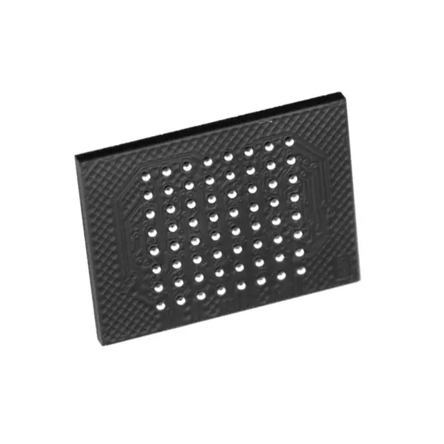
- Part No.:
- XCF128XFTG64C
- Manufacturer:
- AMD
- Category:
- Configuration PROMs for FPGAs
- Package:
- 64-TBGA
- Datasheet:
-
 XCF128XFTG64C.pdf
- Description:
- IC PROM SRL 128M GATE 64-FTBGA
- Quantity:
- Payment:

- Shipping:

Inventory:2,181
Please send an inquiry. Send us your inquiry, and we will respond immediately.
Product details
Overview
XCF128XFTG64C from Xilinx is a 128-Mb in-system programmable NOR flash memory optimized for Virtex-5 and Virtex-6 FPGA configuration via Slave SelectMAP (x16) interface, delivering up to 800 Mb/s bitstream transfer at 50 MHz clock, with 16-bit data bus, READY_WAIT handshake synchronization, and industrial temperature range (–40°C to +85°C). It serves as high-density, single-chip configuration storage in PCI Express endpoint and high-reliability embedded systems.
For engineers reviewing the XCF128XFTG64C datasheet, pinout, applications, or equivalent options, key selection criteria include synchronous burst read performance, BPI-compatible interface timing, FPGA configuration mode compatibility (Slave SelectMAP only), block-level erase endurance (10,000 cycles), and FT64 package mechanical constraints.
Technical Context
The XCF128XFTG64C implements a multi-bank 8-Mb × 16 architecture with 127 main blocks (1 Mb each) and 4 parameter blocks (256 Kb each), enabling concurrent read and program/erase operations across banks. Its synchronous burst read mode powers up by default and supports up to 54 MHz sequential access with automatic suspension/resumption capability.
It integrates dedicated control logic for FPGA configuration handshaking via READY_WAIT (open-drain input/output), uses separate VDD (1.8 V) and VDDQ (2.5 V or 3.3 V) supplies, and supports JEDEC-standard command set with CFI query support for system-level NOR flash compatibility.
Key Specifications
| Parameter | Value and Actual Design Meaning |
|---|---|
| Main Array Capacity | 128 Mb (8 Mb × 16), sufficient to store one full XC5VLX330 bitstream (79.7 Mbits) plus revision backups or firmware code. |
| Data Bus Width | 16-bit parallel interface, enabling x16 SelectMAP configuration without multiplexing or glue logic. |
| Max Configuration Throughput | 800 Mb/s (50 MHz × 16 bits), achieved in Slave SelectMAP mode with external clock - eliminates wait states for high-speed FPGA boot. |
| Endurance | 10,000 program/erase cycles per block, supporting field firmware updates and design iteration in production systems. |
| Operating Temperature | –40°C to +85°C industrial range, validated for use in telecom infrastructure, industrial controllers, and PCIe add-in cards. |
| Power Supplies | VDD = 1.8 V (core), VDDQ = 2.5 V or 3.3 V (I/O), enabling mixed-voltage board integration with Virtex-5/6 FPGAs. |
| Security Features | Factory-programmed 64-bit unique device number + 16×128-bit OTP registers, enabling secure device identification and immutable configuration flags. |
Pinout & Package
Package: FT64 - 64-pin fine-pitch thin-gull-wing package, 10 mm × 13 mm footprint, 1.0 mm pitch, RoHS-compliant.
| Pin/Terminal | Circuit Role | Design Meaning |
|---|---|---|
| A22–A0 | Address Inputs | 23-bit address bus supporting full 128-Mb memory map; latched on L or K edge depending on mode. |
| DQ15–DQ0 | Data I/O / Command Interface | 16-bit bidirectional data path for bitstream reads, register writes, and JEDEC command inputs. |
| E | Chip Enable | Active-low enable controlling internal logic activation and standby current reduction (IDD2). |
| G | Output Enable | Active-low control for data output drivers during read; must be low before first address latch sequence (FALS). |
| W | Write Enable | Latches address/data on rising edge; used with E to initiate command sequences (e.g., program/erase). |
| READY_WAIT | Ready/Wait Handshake | Open-drain I/O requiring external VDDQ pull-up; coordinates FPGA INIT_B release and synchronizes configuration start. |
| RP | Reset Input | Hardware reset forcing all blocks to Locked state and clearing configuration register; drives READY_WAIT low on assertion. |
| WP | Write Protect Input | Hardware lock-down control: VIH enables unlock, VIL disables modification of locked-block protection status. |
| K | Configuration Clock | Synchronizes burst reads in Slave SelectMAP mode; ignored in asynchronous or write operations. |
| L | Latch Enable | Controls address latching timing; must be held VIH during power-up/FALS, toggled for address capture in async mode. |
| VDD / VDDQ / VSS / VSSQ | Power & Ground | Separate core (1.8 V) and I/O (2.5/3.3 V) supplies with dedicated ground returns - critical for signal integrity in high-speed BPI interfaces. |
| VPP | Program Supply / Control | Configurable: low-voltage = hardware write protect; high-voltage = fast-program supply (not required for standard operation). |
Key Features
| Feature | Design Value |
|---|---|
| FPGA Configuration Synchronization | READY_WAIT handshake eliminates timing margin uncertainty between FPGA INIT_B deassertion and flash readiness - reduces boot failure risk in high-reliability systems. |
| MultiBank Dual-Operation Architecture | 16 independent 8-Mb banks allow background erase/program in one bank while reading bitstream from another - enables seamless MultiBoot switching without interrupting active configuration. |
| Standard NOR Flash Interface | Full CFI compliance and JEDEC command set enable reuse of existing NOR flash drivers and bootloader code - no FPGA-side firmware changes needed for data storage access. |
| Industrial Temperature Operation | Guaranteed functionality from –40°C to +85°C without derating - qualified for deployment in uncontrolled environments like base station cabinets or factory-floor controllers. |
| OTP Security Registers | 17 programmable registers (16×128-bit + 2×64-bit), including factory-unique 64-bit ID, provide tamper-resistant storage for calibration data, licensing keys, or secure boot flags. |
Applications
| PCI Express Endpoint Boot | Virtex-6 FPGA Configuration |
|---|---|
Use Scenario: High-speed add-in card (e.g., video capture or signal processing) requiring sub-100 ms FPGA reconfiguration after hot-plug or firmware update. IC Role / Device Role / Timing Role: Primary configuration storage delivering bitstream via Slave SelectMAP x16 interface synchronized by READY_WAIT to FPGA INIT_B. Use Value: 800 Mb/s throughput enables full XC6VLX365T bitstream load in <95 ms - meets PCIe 2.0/3.0 enumeration timing budgets. |
Use Scenario: Industrial vision system using Virtex-6 LX240T FPGA with dual bitstream fallback for fail-safe operation during field upgrades. IC Role / Device Role / Timing Role: Non-volatile configuration source supporting MultiBoot addressing and parameter block storage for revision metadata. Use Value: 4×256-Kb parameter blocks hold version IDs and checksums; 127×1-Mb main blocks store primary/fallback bitstreams with independent lock control. |
| Telecom Line Card Initialization | Defense Avionics Reconfiguration |
Use Scenario: Carrier-grade optical transport module requiring deterministic, radiation-tolerant boot within 200 ms after power cycle. IC Role / Device Role / Timing Role: Single-chip configuration solution replacing legacy parallel PROM + CPLD glue logic; READY_WAIT ensures FPGA starts config only after flash is ready. Use Value: Eliminates external timing components and reduces BOM count by 3+ parts while maintaining -40°C to +85°C operation. |
Use Scenario: Radar processing unit needing secure, authenticated FPGA configuration with anti-tamper traceability. IC Role / Device Role / Timing Role: Secure boot enabler storing encrypted bitstream headers and OTP-based cryptographic keys in protected registers. Use Value: Factory-programmed 64-bit unique ID + 16×128-bit OTP registers enable device-specific key binding and firmware chain-of-custody logging. |
Equivalent & Alternatives
The following parts are listed as comparable options for similar FPGA configuration storage applications.
| Alternative Part | Technical Difference | Application Difference | Selection Advice |
|---|---|---|---|
| XCF32PFTG64C | 32-Mb capacity, same FT64 package, identical pinout and timing - but lower bandwidth (248 Mb/s max) and no MultiBoot parameter block support. | Suitable only for smaller Virtex-5 designs (e.g., XC5VLX50); cannot store multiple revisions or large Virtex-6 bitstreams. | Select when cost sensitivity outweighs need for revision storage or PCIe endpoint speed. |
| MT28EW128ABA1HPC-0SIT | 128-Mb Micron Parallel NOR flash, 16-bit bus, CFI-compliant, but lacks READY_WAIT, FPGA-specific command set, and MultiBoot support. | Requires FPGA-side logic for configuration sequencing; not validated for Virtex-5/6 SelectMAP - needs custom driver development. | Choose only if migrating from generic NOR flash and willing to implement custom configuration state machine in FPGA fabric. |
Compared with XCF128XFTG64C, the XCF32PFTG64C offers pin-compatible downsizing for cost-sensitive Virtex-5 applications, while the MT28EW128ABA1HPC-0SIT provides raw NOR density without FPGA-optimized handshaking - making XCF128XFTG64C the only solution delivering guaranteed 800 Mb/s, READY_WAIT synchronization, and MultiBoot out-of-box.
Availability
XCF128XFTG64C is available at Aetrix Electronics and suitable for PCI Express endpoint boot, Virtex-6 FPGA configuration, telecom line card initialization, and defense avionics reconfiguration requiring stable component supply across extended product lifecycles.
Supply support for XCF128XFTG64C includes scheduled delivery planning, volume procurement assistance, BOM continuity management, traceable sourcing, and lifecycle availability coordination for OEM customers, industrial embedded developers, connected-device designers, and electronics production programs.
Manufacturer
Xilinx (now part of AMD) is a fabless semiconductor company specializing in programmable logic devices, FPGA architectures, and configurable system-on-chip solutions for high-performance computing and adaptive hardware acceleration.
The Platform Flash XL product line was designed specifically to eliminate configuration bottlenecks in Virtex-5 and Virtex-6 systems - integrating FPGA-aware timing, handshaking, and MultiBoot features into a single NOR flash die.
FAQ
Is XCF128XFTG64C compatible with Virtex-7 or UltraScale FPGAs?
No. XCF128XFTG64C is explicitly supported only for Virtex-5 and Virtex-6 FPGAs per DS617 documentation. It lacks the command set, timing parameters, and configuration mode support required for Virtex-7 or UltraScale families. Using it with newer FPGAs may result in failed configuration or undefined behavior. For Virtex-7/UltraScale, Xilinx specifies different configuration PROMs such as the XCFxxS series or QSPI-based solutions.
What is the purpose of the READY_WAIT pin on XCF128XFTG64C?
The READY_WAIT pin on XCF128XFTG64C provides hardware synchronization between the flash and FPGA during configuration startup. By default, it operates as an open-drain input pulled high externally; the device drives it low during reset and releases it upon readiness. When wired to the FPGA's INIT_B pin, it forms a wired-AND handshake ensuring the FPGA does not begin configuration until the XCF128XFTG64C is fully initialized and ready to deliver valid data.
Can XCF128XFTG64C be programmed directly via JTAG without an FPGA present?
No. XCF128XFTG64C does not have a native JTAG interface. Programming requires indirect in-system programming via a connected Virtex-5 or Virtex-6 FPGA using Xilinx iMPACT software and a JTAG cable. The FPGA acts as a bridge, loading an in-system programming engine that controls the XCF128XFTG64C's BPI interface. Standalone programmers must use third-party gang programmers supporting the BPI protocol and MCS file format.
Does XCF128XFTG64C support simultaneous read and erase operations?
Yes - but only across different banks. The XCF128XFTG64C's 16-bank architecture allows a read operation to proceed in one bank while an erase or program operation executes in another. However, only one bank can be in erase/program mode at any time, and burst reads may cross bank boundaries without interruption. This enables MultiBoot bitstream switching without halting active configuration.
What voltage levels are required for VDDQ on XCF128XFTG64C?
XCF128XFTG64C supports VDDQ at either 2.5 V or 3.3 V, independently of the 1.8 V VDD core supply. The I/O buffers are designed to interface directly with Virtex-5/6 FPGA SelectMAP pins operating at those voltages. Selection is determined by board-level power design - no internal configuration is needed. Both levels are fully characterized in DS617 for timing and drive strength.
XCF128XFTG64C Specifications
- Product attributes
- Attribute value
- Manufacturer:
- AMD
- Series:
- -
- Package/Case:
- 64-TBGA
- Packaging:
- Tray
- Product Status:
- Obsolete
- Programmable:
- Not Verified
- Programmable Type:
- In System Programmable
- Memory Size:
- 128Mb
- Voltage - Supply:
- 1.7V ~ 2V
- Operating Temperature:
- -40°C ~ 85°C
- Mounting Type:
- Surface Mount
- Supplier Device Package:
- 64-FTBGA (10x13)
XCF128XFTG64C FAQ
1.How can I place an order for XCF128XFTG64C through Aetrix?
Please submit a Request for Quotation (RFQ) for XCF128XFTG64C on Aetrix. Our sales agent will provide a competitive quotation and guide you through the order confirmation once you accept the terms.
2.Are the price and stock information for XCF128XFTG64C reliable?
The price and inventory of XCF128XFTG64C are updated periodically and may fluctuate due to market conditions. Stock and pricing data are typically refreshed every 24 hours. Quotation validity for XCF128XFTG64C is usually 5 days.
3.What payment methods are accepted for XCF128XFTG64C?
We accept Wire Transfer, PayPal, Credit Card, Western Union, MoneyGram, and Escrow for XCF128XFTG64C transactions.
Note: Certain payment methods may incur a processing fee.
4.How is shipping managed for XCF128XFTG64C?
XCF128XFTG64C orders can be shipped via leading logistics carriers, including DHL, UPS, FedEx, TNT, or Registered Mail.
Once your XCF128XFTG64C order is processed, you will receive an email with the shipment details and tracking number.
Note: Tracking information may take up to 24 hours to appear. Express delivery typically takes 3–5 business days.
5.How can I obtain technical support or documentation for XCF128XFTG64C?
For technical support, including XCF128XFTG64C datasheets, pinout diagrams, or application guidance, please contact our engineering support team. They can provide detailed documentation and assistance for your XCF128XFTG64C requirements.
6.How does Aetrix verify that XCF128XFTG64C is sourced from the original manufacturer or authorized distributors?
All XCF128XFTG64C products on Aetrix are procured from qualified distributors and authorized channels. Our dedicated quality assurance team conducts strict verification, including traceability checks and, if necessary, third-party testing. This ensures that XCF128XFTG64C meets industry standards.
7.What is the process for return or replacement of XCF128XFTG64C?
All XCF128XFTG64C units undergo pre-shipment inspection (PSI). If there is an issue with XCF128XFTG64C, returns or replacements are accepted under the following conditions:
1.Quantity discrepancies, incorrect items, or visible external defects (such as breakage or corrosion), acknowledged by Aetrix.
2.The issue is reported within 90 days of delivery.
3.The XCF128XFTG64C part is unused and in its original packaging.
Return procedure for XCF128XFTG64C:
1.Submit a request within 90 days.
2.Obtain a Return Material Authorization (RMA) from Aetrix.
XCF128XFTG64C Tags

-
AT17LV512A-10PU
Microchip Technology

-
EPCQ4ASI8N
Intel
-
AT17LV256-10PU
Microchip Technology

-
AT17LV256-10NU
Microchip Technology
-
EPCQ16ASI8N
Intel
-
AT17LV010-10PU
Microchip Technology
-
EPCQ32ASI8N
Intel

-
EPCQ64ASI16N
Intel
-
EPCQ128ASI16N
Intel
-
AT17LV512A-10JU
Microchip Technology
-
AT17LV512-10JU
Microchip Technology
-
AT17LV010-10JU
Microchip Technology
Tech Hub

A practical engineering and sourcing framework covering lifecycle verification, lifetime-buy calculations, replacement qualification, supplier checks and counterfeit-risk controls.

TTL and CMOS logic families differ in thresholds, loading, output drive, power and timing. This engineering guide compares 74HC and 74HCT, calculates noise margins and checks 3.3 V/5 V compatibility.

A practical engineering guide to 3.3V and 5V logic compatibility, input thresholds, resistor dividers, translator ICs, MOSFET level shifting, I2C pull-ups, timing limits and power-sequencing risks.

The 74HC595 uses push-pull logic outputs, while the TPIC6B595 uses 50 V open-drain DMOS sinks for higher-power loads. This guide compares timing, current limits, 3.3 V interfacing, load wiring, thermal…

The 74HC595 converts serial data into eight stable parallel outputs. This guide covers pin functions, shift and storage timing, OE and MR behavior, drive-current limits, cascading, voltage compatibilit…

A technical comparison of level-sensitive latches and edge-triggered flip-flops, covering timing windows, setup and hold limits, master–slave operation, time borrowing, race-through, HDL inference and…

A D latch stores one bit while Enable controls when data can pass. This reference covers gate-level operation, truth tables, transparency, setup and hold timing, LE versus OE, common ICs and practical …

An SR latch stores one bit through cross-coupled feedback. This engineering reference covers NOR and NAND implementations, truth tables, forbidden-state recovery, gated operation, switch debouncing, fa…

Latch circuits retain one bit through feedback. This technical reference covers SR and D latches, truth tables, transparency, timing limits, latch-versus-flip-flop behavior, applications and common log…

An engineering guide to LED driver operation, constant-current and constant-voltage outputs, linear and switching topologies, dimming, IC selection, calculations, replacement compatibility, and fault c…


