
 My Inquiry
 My Account


AMD XCS20XL-4VQG100C
- Part No.:
- XCS20XL-4VQG100C
- Manufacturer:
- AMD
- Category:
- FPGAs (Field Programmable Gate Array)
- Package:
- 100-TQFP
- Datasheet:
-
 XCS20XL-4VQG100C.pdf
- Description:
- IC FPGA 77 I/O 100VQFP
- Quantity:
- Payment:

- Shipping:

Inventory:4,549
Please send an inquiry. Send us your inquiry, and we will respond immediately.
Product details
Overview
XCS20XL-4VQG100C from AMD (formerly Xilinx) is a Spartan-XL family FPGA with 20,000 system gates, 100-pin VQFP package, 4.5 ns typical I/O delay, and -4 speed grade. It serves as a reconfigurable logic fabric for digital control, interface bridging, and glue logic in industrial PLCs and legacy system upgrades.
For engineers reviewing the XCS20XL-4VQG100C datasheet, pinout, applications, or equivalent options, key selection factors include I/O count, propagation delay, configuration mode support, and legacy 3.3 V/5 V mixed-voltage tolerance.
Technical Context
The XCS20XL-4VQG100C implements a segmented interconnect architecture with configurable logic blocks (CLBs), dedicated carry chains, and I/O blocks supporting LVTTL, LVCMOS, and PCI-compliant signaling. It uses SRAM-based configuration with external PROM or microprocessor loading.
It supports in-system programmability via JTAG boundary-scan (IEEE 1149.1) and operates over commercial temperature range (0°C to 70°C). Configuration bitstream is volatile and requires external memory reload on power-up.
Key Specifications
| Parameter | Value and Actual Design Meaning |
|---|---|
| Logic Gates | 20,000 system gates - defines maximum combinational logic capacity for gate-equivalent design mapping |
| Speed Grade | -4 - guarantees ≤4.5 ns CLB-to-CLB propagation delay under worst-case commercial conditions |
| I/O Pins | 84 user I/Os - supports parallel bus interfaces, address/data multiplexing, and multi-protocol signal routing |
| Supply Voltage | 5.0 V core & I/O - enables direct interfacing with legacy TTL/CMOS systems without level-shifting |
| Configuration Mode | Master Serial, Slave Parallel, JTAG - allows flexible programming via microcontroller, FPGA programmer, or boundary-scan test infrastructure |
| Operating Temp | 0°C to +70°C - validated for commercial-grade embedded control and instrumentation environments |
Pinout & Package
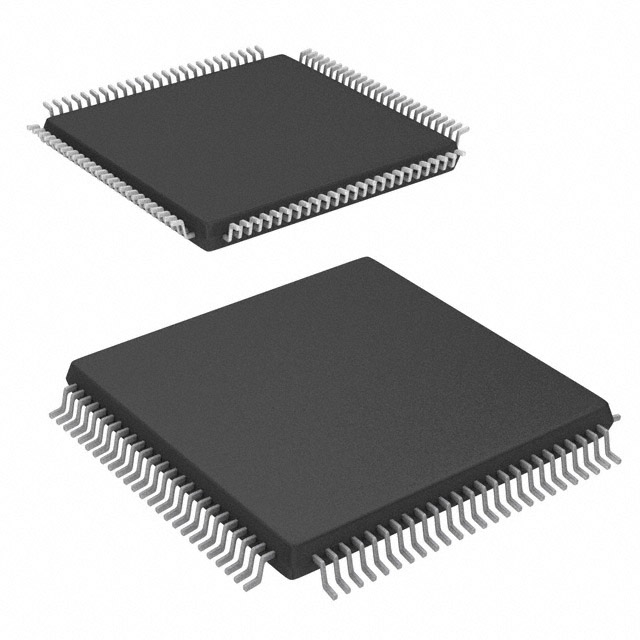
100-pin Very Thin Quad Flat Pack (VQFP), 14 mm × 14 mm body, 0.5 mm pitch, thermally enhanced plastic package with exposed pad not present. RoHS-compliant, lead-free finish.
| Pin/Terminal | Circuit Role | Design Meaning |
|---|---|---|
| GND | Ground reference | Multiple dedicated pins provide low-inductance return paths for I/O and core logic switching currents |
| VCC | Core & I/O supply | 5.0 V supply input shared across internal logic and output drivers; decoupling required per pin group |
| PROGRAM_B | Configuration reset | Active-low asynchronous input that clears configuration memory and initiates reconfiguration sequence |
| DONE | Configuration status | Open-drain output indicating successful configuration completion; pulled high externally to enable startup |
| TCK/TMS/TDI/TDO | JTAG interface | IEEE 1149.1 boundary-scan test and programming interface; supports in-system debug and verification |
Key Features
| Feature | Design Value |
|---|---|
| 5 V tolerant I/Os | Supports direct connection to legacy 5 V buses without external level shifters or voltage translators |
| Configurable I/O standards | Per-pin programmable drive strength, slew rate, and pull-up/pull-down resistors for signal integrity tuning |
| Carry logic chain | Optimized fast arithmetic path enabling efficient counters, adders, and comparators without LUT resource overhead |
| Boundary-scan test support | Full IEEE 1149.1 compliance enables automated PCB test, fault isolation, and in-field reprogramming |
Applications
| Industrial Motion Control | Legacy System Interface Bridge |
|---|---|
Use Scenario: Real-time axis coordination and encoder feedback processing in servo drives with aging microcontrollers. IC Role / Device Role / Timing Role: FPGA logic fabric implementing custom PWM generators, quadrature decoding, and safety interlock state machines. Use Value: Enables deterministic sub-microsecond response latency and field-upgradable control algorithms without board redesign. | Use Scenario: Interfacing modern ARM-based controllers to legacy parallel bus peripherals (e.g., ISA-style data acquisition cards). IC Role / Device Role / Timing Role: Protocol translator and timing adapter between asynchronous 8-bit data strobes and synchronous APB bus cycles. Use Value: Eliminates need for discrete glue logic and reduces BOM count while preserving original timing margins. |
| Test Equipment Signal Generator | Avionics Maintenance Simulator |
Use Scenario: Generating calibrated digital stimulus waveforms (SPI, I²C, custom serial) for IC functional validation. IC Role / Device Role / Timing Role: Reconfigurable pattern generator with precise edge placement and variable clock domain crossing. Use Value: Supports multiple protocol variants via bitstream swap, reducing hardware variants in production test fixtures. | Use Scenario: Simulating ARINC 429 transmitter behavior for ground-based avionics diagnostics. IC Role / Device Role / Timing Role: Deterministic pulse-width modulator with programmable label filtering and parity generation. Use Value: Meets ARINC 429 timing spec (±100 ns pulse width accuracy) using internal carry chains and fixed-delay routing. |
Equivalent & Alternatives
The following parts are listed as comparable options for similar reconfigurable logic applications.
| Alternative Part | Technical Difference | Application Difference | Selection Advice |
|---|---|---|---|
| XCS10XL-4VQG100C | 10,000 system gates, identical pinout and speed grade | Lower logic density limits complex state machines and wide datapaths | Select when design fits within half the gate count and cost reduction is prioritized over future scalability |
| XCS30XL-4VQG100C | 30,000 system gates, same package and I/O structure | Higher gate count supports larger control logic, more concurrent interfaces, or dual-function partitioning | Choose when additional logic resources are needed for feature expansion or redundancy without changing PCB layout |
Compared with XCS10XL-4VQG100C and XCS30XL-4VQG100C, the XCS20XL-4VQG100C provides balanced logic capacity for mid-complexity control tasks while maintaining compatibility with existing 100-pin VQFP footprint and timing constraints.
Availability
XCS20XL-4VQG100C is available at Aetrix Electronics and suitable for industrial motion control, legacy interface bridging, and test equipment signal generation requiring stable component supply and long-term obsolescence management.
Supply support for XCS20XL-4VQG100C includes scheduled delivery planning, volume procurement assistance, BOM continuity management, traceable sourcing, and lifecycle availability coordination for OEM customers, industrial embedded developers, connected-device designers, and electronics production programs.
Manufacturer
AMD is a global semiconductor company delivering adaptive computing, graphics, and visualization technologies for data center, client, and embedded markets.
The Spartan-XL family was designed for cost-sensitive, high-volume applications requiring reliable reconfigurable logic with 5 V compatibility and simple configuration flow.
FAQ
What is the configuration method supported by XCS20XL-4VQG100C?
The XCS20XL-4VQG100C supports Master Serial, Slave Parallel, and JTAG configuration modes. It loads its bitstream from external PROM or microprocessor-controlled memory. JTAG enables boundary-scan testing and in-system programming without requiring dedicated configuration hardware. The XCS20XL-4VQG100C does not support internal nonvolatile configuration storage.
Does XCS20XL-4VQG100C support 3.3 V I/O operation?
No, the XCS20XL-4VQG100C is a 5 V-only device. Its I/O buffers are designed for 5 V TTL/CMOS signaling levels and are not 3.3 V tolerant. Using 3.3 V signals directly may cause damage or unreliable operation. Level translation is required when interfacing with 3.3 V systems. The XCS20XL-4VQG100C specification explicitly defines VCCIO = 5.0 V ±5%.
What is the maximum operating frequency of logic implemented in XCS20XL-4VQG100C?
The XCS20XL-4VQG100C has a -4 speed grade specifying ≤4.5 ns CLB-to-CLB propagation delay under worst-case commercial conditions. Achievable system clock frequencies depend on design topology but typically range up to 125 MHz for fully pipelined register-to-register paths. The XCS20XL-4VQG100C datasheet provides timing analysis tools and delay matrices for accurate path-based estimation.
Is XCS20XL-4VQG100C pin-compatible with newer Spartan families?
No, the XCS20XL-4VQG100C is not pin-compatible with Spartan-II, Spartan-3, or later families. Differences in power pin allocation, configuration pin functions, and I/O bank organization prevent direct replacement. Migration requires PCB redesign and logic re-synthesis. The XCS20XL-4VQG100C remains a standalone solution for legacy 5 V system maintenance.
What thermal considerations apply to XCS20XL-4VQG100C in continuous operation?
The XCS20XL-4VQG100C has no integrated thermal sensor and relies on ambient convection cooling. Its 100-pin VQFP package exhibits a θJA of 45°C/W. For continuous operation at full utilization, board-level thermal design must maintain junction temperature below 125°C. The XCS20XL-4VQG100C datasheet specifies derating curves for power dissipation versus ambient temperature and airflow.
XCS20XL-4VQG100C Specifications
- Product attributes
- Attribute value
- Manufacturer:
- AMD
- Series:
- Spartan®-XL
- Package/Case:
- 100-TQFP
- Packaging:
- Tray
- Product Status:
- Obsolete
- Programmable:
- Not Verified
- Number of LABs/CLBs:
- 400
- Number of Logic Elements/Cells:
- 950
- Total RAM Bits:
- 12800
- Number of I/O:
- 77
- Number of Gates:
- 20000
- Voltage - Supply:
- 3V ~ 3.6V
- Mounting Type:
- Surface Mount
- Operating Temperature:
- 0°C ~ 85°C (TJ)
- Grade:
- -
- Qualification:
- -
- Supplier Device Package:
- 100-VQFP (14x14)
XCS20XL-4VQG100C FAQ
1.How can I place an order for XCS20XL-4VQG100C through Aetrix?
Please submit a Request for Quotation (RFQ) for XCS20XL-4VQG100C on Aetrix. Our sales agent will provide a competitive quotation and guide you through the order confirmation once you accept the terms.
2.Are the price and stock information for XCS20XL-4VQG100C reliable?
The price and inventory of XCS20XL-4VQG100C are updated periodically and may fluctuate due to market conditions. Stock and pricing data are typically refreshed every 24 hours. Quotation validity for XCS20XL-4VQG100C is usually 5 days.
3.What payment methods are accepted for XCS20XL-4VQG100C?
We accept Wire Transfer, PayPal, Credit Card, Western Union, MoneyGram, and Escrow for XCS20XL-4VQG100C transactions.
Note: Certain payment methods may incur a processing fee.
4.How is shipping managed for XCS20XL-4VQG100C?
XCS20XL-4VQG100C orders can be shipped via leading logistics carriers, including DHL, UPS, FedEx, TNT, or Registered Mail.
Once your XCS20XL-4VQG100C order is processed, you will receive an email with the shipment details and tracking number.
Note: Tracking information may take up to 24 hours to appear. Express delivery typically takes 3–5 business days.
5.How can I obtain technical support or documentation for XCS20XL-4VQG100C?
For technical support, including XCS20XL-4VQG100C datasheets, pinout diagrams, or application guidance, please contact our engineering support team. They can provide detailed documentation and assistance for your XCS20XL-4VQG100C requirements.
6.How does Aetrix verify that XCS20XL-4VQG100C is sourced from the original manufacturer or authorized distributors?
All XCS20XL-4VQG100C products on Aetrix are procured from qualified distributors and authorized channels. Our dedicated quality assurance team conducts strict verification, including traceability checks and, if necessary, third-party testing. This ensures that XCS20XL-4VQG100C meets industry standards.
7.What is the process for return or replacement of XCS20XL-4VQG100C?
All XCS20XL-4VQG100C units undergo pre-shipment inspection (PSI). If there is an issue with XCS20XL-4VQG100C, returns or replacements are accepted under the following conditions:
1.Quantity discrepancies, incorrect items, or visible external defects (such as breakage or corrosion), acknowledged by Aetrix.
2.The issue is reported within 90 days of delivery.
3.The XCS20XL-4VQG100C part is unused and in its original packaging.
Return procedure for XCS20XL-4VQG100C:
1.Submit a request within 90 days.
2.Obtain a Return Material Authorization (RMA) from Aetrix.
XCS20XL-4VQG100C Tags
-
ICE40LP384-SG32
Lattice Semiconductor Corporation
-
ICE40UL640-CM36AI
Lattice Semiconductor Corporation
-
ICE40UL1K-CM36AI
Lattice Semiconductor Corporation
-
LCMXO2-256HC-4SG32C
Lattice Semiconductor Corporation
-
10M02DCV36C8G
Intel
-
LCMXO2-256HC-4SG32I
Lattice Semiconductor Corporation
-
ICE5LP1K-SG48ITR
Lattice Semiconductor Corporation
-
ICE40LP1K-CM36
Lattice Semiconductor Corporation
-
LCMXO2-256ZE-1SG32I
Lattice Semiconductor Corporation
-
LCMXO2-256HC-4SG48I
Lattice Semiconductor Corporation
-
ICE40LP1K-CM81
Lattice Semiconductor Corporation

-
T20W80I4
Efinix, Inc.
Tech Hub

A practical engineering and sourcing framework covering lifecycle verification, lifetime-buy calculations, replacement qualification, supplier checks and counterfeit-risk controls.

TTL and CMOS logic families differ in thresholds, loading, output drive, power and timing. This engineering guide compares 74HC and 74HCT, calculates noise margins and checks 3.3 V/5 V compatibility.

A practical engineering guide to 3.3V and 5V logic compatibility, input thresholds, resistor dividers, translator ICs, MOSFET level shifting, I2C pull-ups, timing limits and power-sequencing risks.

The 74HC595 uses push-pull logic outputs, while the TPIC6B595 uses 50 V open-drain DMOS sinks for higher-power loads. This guide compares timing, current limits, 3.3 V interfacing, load wiring, thermal…

The 74HC595 converts serial data into eight stable parallel outputs. This guide covers pin functions, shift and storage timing, OE and MR behavior, drive-current limits, cascading, voltage compatibilit…

A technical comparison of level-sensitive latches and edge-triggered flip-flops, covering timing windows, setup and hold limits, master–slave operation, time borrowing, race-through, HDL inference and…

A D latch stores one bit while Enable controls when data can pass. This reference covers gate-level operation, truth tables, transparency, setup and hold timing, LE versus OE, common ICs and practical …

An SR latch stores one bit through cross-coupled feedback. This engineering reference covers NOR and NAND implementations, truth tables, forbidden-state recovery, gated operation, switch debouncing, fa…

Latch circuits retain one bit through feedback. This technical reference covers SR and D latches, truth tables, transparency, timing limits, latch-versus-flip-flop behavior, applications and common log…

An engineering guide to LED driver operation, constant-current and constant-voltage outputs, linear and switching topologies, dimming, IC selection, calculations, replacement compatibility, and fault c…


