
 My Inquiry
 My Account


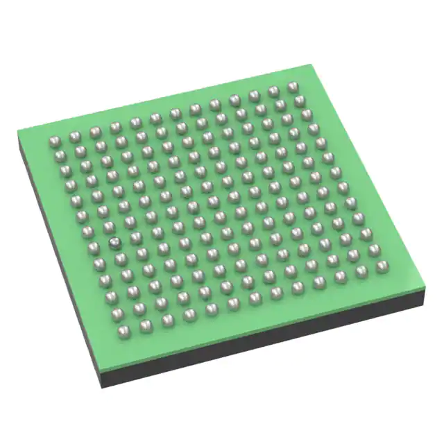
Texas Instruments XIO2001ZWS
- Part No.:
- XIO2001ZWS
- Manufacturer:
- Texas Instruments
- Category:
- Specialized
- Package:
- 169-LFBGA
- Datasheet:
-
 XIO2001ZWS.pdf
- Description:
- PCI EXPRESS (PCIE) TO PCI B
- Quantity:
- Payment:

- Shipping:

Inventory:1,130
Please send an inquiry. Send us your inquiry, and we will respond immediately.
Product details
Overview
XIO2001ZWS from Texas Instruments is a single-function PCI Express to PCI bus translation bridge compliant with PCI Express Base Specification 2.0 and PCI Express to PCI/PCI-X Bridge Specification 1.0. It provides full ×1 PCIe throughput (250 MB/s bidirectional), supports 66-MHz/32-bit PCI local bus operation, and integrates an internal arbiter for up to six external PCI masters - enabling legacy PCI add-in cards in modern PCIe-based enterprise servers and industrial control systems.
For engineers reviewing the XIO2001ZWS datasheet, XIO2001ZWS pinout, XIO2001ZWS application, or XIO2001ZWS equivalent, this device serves as a critical interconnect solution where backward compatibility with 32-bit PCI peripherals is required without redesigning host infrastructure - especially in data center server expansion slots, factory automation backplanes, and ruggedized PC-based controllers.
Technical Context
The XIO2001ZWS implements a robust pipeline architecture to minimize transaction latency between its PCIe ×1 upstream interface and downstream 32-bit PCI bus. It supports simultaneous handling of eight posted and four non-posted transactions downstream, and six posted and four non-posted upstream - preserving bandwidth under mixed memory-mapped I/O and configuration access loads.
Its dual-clock domain design isolates the 100-MHz differential (or 125-MHz single-ended) PCIe reference clock from the configurable 25/33/50/66-MHz PCI bus clocks. Power management includes L0s/L1 active-state link power management, D1/D2/D3hot/D3cold states, and PCI Express Advanced Error Reporting with ECRC support - all implemented in hardware without firmware dependency for basic operation.
Key Specifications
| Parameter | Value and Actual Design Meaning |
|---|---|
| PCIe Interface | ×1 lane, PCIe Base Spec 2.0 compliant, 250 MB/s bidirectional throughput - enables direct attachment to root complex or switch upstream port. |
| PCI Bus Interface | 32-bit, 66-MHz max (33/25 MHz at 5.0 V), PCI Local Bus Spec 2.3 compliant - supports legacy add-in cards including RAID controllers and I/O expansion modules. |
| Transaction Support | Downstream: 8 posted + 4 non-posted; Upstream: 6 posted + 4 non-posted - ensures high concurrency for burst transfers and split transactions in multi-master environments. |
| Power Management | D1/D2/D3hot/D3cold states + L0s/L1 ASPM - reduces system idle power by gating clocks and lowering link activity without software intervention. |
| Reference Clock | 100-MHz differential common-ref or 125-MHz single-ended - selectable via REFCLK125_SEL pin; supports spread spectrum for EMI reduction. |
| PCI Clock Outputs | Six buffered outputs (25/33/50/66 MHz) - eliminates need for external clock buffers when driving multiple PCI slots or peripherals. |
| I/O Voltage Tolerance | PCI bus: 3.3-V or 5.0-V (25/33 MHz only at 5.0 V); I/Os: 3.3-V LVCMOS - enables interoperability with both modern low-voltage and legacy 5-V PCI devices. |
Pinout & Package
Package: 169-ball ZWS nFBGA (12.00 mm × 12.00 mm), lead-free, RoHS-compliant.
| Pin/Terminal | Circuit Role | Design Meaning |
|---|---|---|
| RXP / RXN | PCIe Differential Receive Input | High-speed input pair for PCIe ×1 lane; requires controlled 100-Ω differential impedance trace routing. |
| TXP / TXN | PCIe Differential Transmit Output | High-speed output pair; series AC-coupling capacitors required per PCIe spec before connector. |
| REFCLK+ / REFCLK− | Differential Reference Clock Input | Accepts 100-MHz differential reference; if single-ended 125-MHz used, REFCLK− must be AC-coupled to ground. |
| PERST | PCIe Reset Input | Asynchronous active-low reset with hysteresis; asserts internal POR when system power stabilizes. |
| CLKREQ | PCIe Clock Request Output | Open-drain signal requesting upstream clock resumption during L1 exit; requires external pullup. |
| WAKE | PCIe Wake Signal Output | Active-low open-drain output to reactivate main power rails and reference clocks; requires external pullup. |
| AD[31:0] | PCI Address/Data Multiplexed Bus | 32-bit time-multiplexed address/data lines; driven by bridge during configuration cycles and memory/I/O reads/writes. |
| C/BE[3:0]# | PCI Command/Byte Enable | Four active-low signals encoding PCI command type (MEM, I/O, CONFIG) and byte enables for 32-bit transfers. |
| FRAME#, IRDY#, TRDY#, DEVSEL# | PCI Transaction Control | Core handshake signals defining transaction initiation, initiator/target readiness, and device selection timing. |
| REQ[5:0] / GNT[5:0] | PCI Arbitration Interface | Supports up to six external PCI masters; internal arbiter prioritizes requests with configurable 2-level scheme. |
| GPIO0–GPIO4 | Multi-function I/O Terminals | Five 3.3-V LVCMOS pins usable as GPIOs or dedicated functions (CLKRUN, PWR_OVRD, SDA/SCL). |
Key Features
| Feature | Design Value |
|---|---|
| PCIe-to-PCI Translation | Hardware-accelerated protocol conversion with no driver or OS modification required for legacy PCI devices. |
| Advanced Error Reporting | Includes ECRC generation/checking and error forwarding (PCIe data poisoning, PCI parity errors) for system-level fault isolation. |
| Configurable PCI Clock Outputs | Six independent clock outputs (25/33/50/66 MHz) with programmable frequency selection - simplifies timing design across multi-slot backplanes. |
| Internal Arbiter with Prioritization | Supports six external PCI masters with 2-level internal prioritization - eliminates need for external arbitration logic in compact designs. |
| JTAG/BS Boundary Scan | Fully IEEE 1149.1-compliant test interface with TRST, TCK, TMS, TDI, TDO - enables production test and debug without intrusive probing. |
| AUX Power Switch Integration | Integrated VAUX drain switch activates only when main power is off - prevents auxiliary rail leakage and meets PCI power budget requirements. |
Applications
| Enterprise Server Expansion | Industrial Backplane Interconnect |
|---|---|
|
Use Scenario: Adding legacy PCI-based RAID or FPGA co-processor cards into modern PCIe-based rack-mount servers. IC Role / Device Role / Timing Role: Acts as protocol translator and timing bridge between PCIe root complex and 32-bit PCI bus segment. Use Value: Enables reuse of certified, field-proven PCI peripherals without redesigning motherboard or BIOS - reducing qualification time and cost. |
Use Scenario: Integrating legacy motion control or analog I/O modules into a new PCIe-based industrial controller backplane. IC Role / Device Role / Timing Role: Provides deterministic, low-latency bridging with configurable 66-MHz PCI clock outputs synchronized to system reference. Use Value: Maintains real-time determinism for time-critical I/O while supporting hot-plug-capable PCI slots via PERST/WAKE signaling. |
| PC-Based Factory Automation | Retail Payment Terminal Upgrade |
|
Use Scenario: Retrofitting older PC-based PLCs with PCIe motherboards while retaining existing PCI data acquisition cards. IC Role / Device Role / Timing Role: Serves as transparent bus bridge with full PCI 2.3 compliance, including LOCK and PAR support for atomic operations. Use Value: Preserves investment in calibrated sensor interfaces and custom drivers - no revalidation of measurement accuracy required. |
Use Scenario: Modernizing PCI-based EMV payment terminals with PCIe host platforms while maintaining PCI PTS-certified card readers. IC Role / Device Role / Timing Role: Delivers secure, isolated PCI bus segment with D3cold support for zero-power sleep between transactions. Use Value: Meets PCI PTS power and security requirements without compromising certification status of legacy peripheral stack. |
Equivalent & Alternatives
The following parts are listed as comparable options for similar PCI Express to PCI bridge applications.
| Alternative Part | Technical Difference | Application Difference | Selection Advice |
|---|---|---|---|
| PLX Technology PEX8112-AB50BCF | PCIe ×1 to PCI-X 133-MHz bridge; supports 64-bit/133-MHz PCI-X; larger 256-pin PBGA package; higher power consumption. | Targeted at high-bandwidth storage or networking where PCI-X bandwidth exceeds 32-bit PCI limits. | Select only if 133-MHz PCI-X or 64-bit addressing is required; not drop-in compatible due to pinout and register map differences. |
| Pericom PI7C9X110BNDE | PCIe ×1 to PCI 32-bit/66-MHz bridge; supports same clock outputs and JTAG; smaller 128-pin TQFP package; lacks ECRC and advanced ASPM. | Suitable for cost-sensitive embedded applications where full PCIe 2.0 AER and L1 ASPM are not mandatory. | Consider for simpler designs needing basic bridging; verify thermal performance - lower thermal dissipation rating than XIO2001ZWS. |
Compared with PEX8112-AB50BCF and PI7C9X110BNDE, the XIO2001ZWS delivers balanced feature depth - including ECRC, L0s/L1 ASPM, and integrated AUX power switching - within a compact 169-ball nFBGA footprint optimized for space-constrained server mezzanine and industrial control modules.
Availability
XIO2001ZWS is available at Aetrix Electronics and suitable for enterprise server expansion, industrial backplane interconnect, and PC-based factory automation requiring stable component supply and long-term lifecycle assurance.
Supply support for XIO2001ZWS includes scheduled delivery planning, volume procurement assistance, BOM continuity management, traceable sourcing, and lifecycle availability coordination for OEM customers, industrial embedded developers, connected-device designers, and electronics production programs.
Manufacturer
Texas Instruments is a global semiconductor leader focused on analog, embedded processing, and connectivity technologies, serving industrial, automotive, and communications markets with high-reliability silicon solutions.
The XIO2001ZWS belongs to TI's PCI Express bridge product line, designed specifically to extend the life of legacy PCI peripherals in next-generation PCIe infrastructure - emphasizing protocol fidelity, power efficiency, and seamless integration into enterprise and industrial platforms.
FAQ
What is the primary function of the XIO2001ZWS?
The XIO2001ZWS is a single-function PCI Express to PCI bus translation bridge that enables legacy 32-bit PCI add-in cards to operate in modern PCIe-based systems. It handles protocol conversion, timing synchronization, and arbitration between the PCIe ×1 upstream interface and downstream PCI bus - all in hardware without requiring driver modifications. The XIO2001ZWS maintains full compliance with PCI Express Base Specification 2.0 and PCI Local Bus Specification 2.3.
Does the XIO2001ZWS support 66-MHz PCI bus operation?
Yes, the XIO2001ZWS supports 66-MHz PCI bus operation when M66EN is asserted high and PCLK66_SEL is configured appropriately. It also supports 25/33/50 MHz modes depending on voltage and configuration. At 5.0 V, only 25 MHz and 33 MHz are allowed per PCI specification - the XIO2001ZWS enforces this constraint through its internal logic and pin strapping. The XIO2001ZWS provides six buffered clock outputs to drive multiple PCI slots synchronously.
How does the XIO2001ZWS handle PCIe power management states?
The XIO2001ZWS supports D1, D2, D3hot, and D3cold device states, plus L0s and L1 Active-State Power Management (ASPM) for the PCIe link. It automatically enters L0s/L1 when packet activity ceases and exits on request via CLKREQ or WAKE. D3cold disables main power while retaining VAUX for wake event detection. The XIO2001ZWS implements these states in hardware - no firmware or software initialization is needed for basic entry/exit behavior.
Can the XIO2001ZWS be used with a 5.0-V PCI bus?
Yes, the XIO2001ZWS supports 5.0-V PCI bus signaling at 25 MHz and 33 MHz only - consistent with PCI Local Bus Specification 2.3. Its PCIR pins accept either 3.3-V or 5.0-V clamp rail voltages, and internal I/O buffers tolerate both levels. However, 66-MHz operation is restricted to 3.3-V PCI bus configurations. The XIO2001ZWS must be configured with appropriate PCIR resistor values and voltage rails to ensure safe 5.0-V interoperability.
What are the key differences between the ZWS and ZAJ nFBGA packages for the XIO2001ZWS?
The XIO2001ZWS ZWS package is a 169-ball nFBGA (12.00 mm × 12.00 mm), while the ZAJ variant is a 144-ball nFBGA (7.00 mm × 7.00 mm). Both are laminate-based, datasheet-equivalent electrically and footprint-compatible with their predecessor MicroStar Jr. BGA packages. The ZWS offers more I/Os and enhanced thermal performance due to larger die pad area - making it preferred for high-throughput or thermally constrained applications. The XIO2001ZWS ZWS pinout differs significantly from ZAJ, particularly in power distribution and clock routing.
XIO2001ZWS Specifications
- Product attributes
- Attribute value
- Manufacturer:
- Texas Instruments
- Series:
- -
- Package/Case:
- 169-LFBGA
- Packaging:
- Tray
- Product Status:
- Active
- Applications:
- PCI Express to PCI Translation Bridge
- Interface:
- PCI Express
- Voltage - Supply:
- 1.35V ~ 1.65V, 3V ~ 3.6V
- Supplier Device Package:
- 169-NFBGA (12x12)
- Grade:
- -
- Qualification:
- -
- Mounting Type:
- Surface Mount
XIO2001ZWS FAQ
1.How can I place an order for XIO2001ZWS through Aetrix?
Please submit a Request for Quotation (RFQ) for XIO2001ZWS on Aetrix. Our sales agent will provide a competitive quotation and guide you through the order confirmation once you accept the terms.
2.Are the price and stock information for XIO2001ZWS reliable?
The price and inventory of XIO2001ZWS are updated periodically and may fluctuate due to market conditions. Stock and pricing data are typically refreshed every 24 hours. Quotation validity for XIO2001ZWS is usually 5 days.
3.What payment methods are accepted for XIO2001ZWS?
We accept Wire Transfer, PayPal, Credit Card, Western Union, MoneyGram, and Escrow for XIO2001ZWS transactions.
Note: Certain payment methods may incur a processing fee.
4.How is shipping managed for XIO2001ZWS?
XIO2001ZWS orders can be shipped via leading logistics carriers, including DHL, UPS, FedEx, TNT, or Registered Mail.
Once your XIO2001ZWS order is processed, you will receive an email with the shipment details and tracking number.
Note: Tracking information may take up to 24 hours to appear. Express delivery typically takes 3–5 business days.
5.How can I obtain technical support or documentation for XIO2001ZWS?
For technical support, including XIO2001ZWS datasheets, pinout diagrams, or application guidance, please contact our engineering support team. They can provide detailed documentation and assistance for your XIO2001ZWS requirements.
6.How does Aetrix verify that XIO2001ZWS is sourced from the original manufacturer or authorized distributors?
All XIO2001ZWS products on Aetrix are procured from qualified distributors and authorized channels. Our dedicated quality assurance team conducts strict verification, including traceability checks and, if necessary, third-party testing. This ensures that XIO2001ZWS meets industry standards.
7.What is the process for return or replacement of XIO2001ZWS?
All XIO2001ZWS units undergo pre-shipment inspection (PSI). If there is an issue with XIO2001ZWS, returns or replacements are accepted under the following conditions:
1.Quantity discrepancies, incorrect items, or visible external defects (such as breakage or corrosion), acknowledged by Aetrix.
2.The issue is reported within 90 days of delivery.
3.The XIO2001ZWS part is unused and in its original packaging.
Return procedure for XIO2001ZWS:
1.Submit a request within 90 days.
2.Obtain a Return Material Authorization (RMA) from Aetrix.
XIO2001ZWS Tags

-
NVT4857UKAZ
NXP Semiconductors

-
TCA8418RTWR
Texas Instruments

-
PCA9546APWR
Texas Instruments

-
MD0100N8-G
Microchip Technology

-
PCA9548APW,118
NXP Semiconductors

-
PCA9540BDP,118
NXP Semiconductors

-
PCA9548APWR
Texas Instruments

-
PCA9546APW,118
NXP Semiconductors

-
PTN3360DBS,518
NXP Semiconductors

-
PCA9546ABS,118
NXP Semiconductors

-
PCA9518PWR
Texas Instruments

-
PCA9545APW,118
NXP Semiconductors
Tech Hub

A practical engineering guide to 3.3V and 5V logic compatibility, input thresholds, resistor dividers, translator ICs, MOSFET level shifting, I2C pull-ups, timing limits and power-sequencing risks.

The 74HC595 uses push-pull logic outputs, while the TPIC6B595 uses 50 V open-drain DMOS sinks for higher-power loads. This guide compares timing, current limits, 3.3 V interfacing, load wiring, thermal…

The 74HC595 converts serial data into eight stable parallel outputs. This guide covers pin functions, shift and storage timing, OE and MR behavior, drive-current limits, cascading, voltage compatibilit…

A technical comparison of level-sensitive latches and edge-triggered flip-flops, covering timing windows, setup and hold limits, master–slave operation, time borrowing, race-through, HDL inference and…

A D latch stores one bit while Enable controls when data can pass. This reference covers gate-level operation, truth tables, transparency, setup and hold timing, LE versus OE, common ICs and practical …

An SR latch stores one bit through cross-coupled feedback. This engineering reference covers NOR and NAND implementations, truth tables, forbidden-state recovery, gated operation, switch debouncing, fa…

Latch circuits retain one bit through feedback. This technical reference covers SR and D latches, truth tables, transparency, timing limits, latch-versus-flip-flop behavior, applications and common log…

An engineering guide to LED driver operation, constant-current and constant-voltage outputs, linear and switching topologies, dimming, IC selection, calculations, replacement compatibility, and fault c…

Operational amplifier guide covering op amp basics, feedback, ideal vs real op amps, common configurations, buffer circuits, offset, bias current, gain-bandwidth, slew rate, rail-to-rail limits and sel…

Jumper cables guide covering safe connection order, red and black clamp placement, final ground connection, cable gauge, length, clamp quality, copper vs CCA cables, jump starter comparison and battery…


