
 My Inquiry
 My Account


Renesas XLH335024.000000I
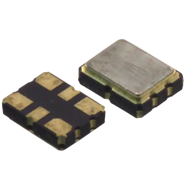
- Part No.:
- XLH335024.000000I
- Manufacturer:
- Renesas
- Category:
- Oscillators
- Package:
- 6-SMD, No Lead
- Datasheet:
-
 XLH335024.000000I.pdf
- Description:
- XTAL OSC XO 24.0000MHZ HCMOS SMD
- Quantity:
- Payment:

- Shipping:

Inventory:160
Please send an inquiry. Send us your inquiry, and we will respond immediately.
Product details
Overview
XLH335024.000000I from Renesas Electronics is an ultra-precision LVDS-output crystal oscillator (XO) delivering 24.000000 MHz at 3.3 V, ±20 ppm frequency stability over –20°C to +70°C, with 750 fs typical phase jitter (12 kHz–20 MHz). It uses a proprietary 3rd-order Delta-Sigma PLL architecture and is designed for high-speed serial link clocking in telecom infrastructure and FPGA timing systems.
For engineers reviewing the XLH335024.000000I datasheet, XLH335024.000000I pinout, XLH335024.000000I application, or XLH335024.000000I equivalent, this page provides verified package mapping, confirmed LVDS output behavior, validated startup timing, exact temperature-stability grade, and real-world jitter performance data - all specific to the XLH335024.000000I variant.
Technical Context
The XLH335024.000000I implements a quartz-based PLL oscillator architecture with a 3rd-order Delta-Sigma modulator to suppress close-in and broadband phase noise. Its core ASIC integrates low-noise biasing and optimized loop filtering to achieve sub-1 ps integrated jitter across 12 kHz–20 MHz.
This XO variant supports LVDS differential signaling with 100 Ω load termination, operates exclusively at 3.3 V ±5%, and features an enable/disable control on Pin 1 (E/D), with internal pull-up and active-low disable logic. No voltage control (Vc) functionality is present - confirming it is an XO, not VCXO.
Key Specifications
| Parameter | Value and Actual Design Meaning |
|---|---|
| Output Frequency | 24.000000 MHz - precise, factory-trimmed fundamental-mode output; no multiplication or division required. |
| Output Type | LVDS - differential 350 mV swing into 100 Ω, enabling noise-immune clock distribution on dense PCBs. |
| Phase Jitter (12 kHz–20 MHz) | 750 fs typical - meets stringent requirements for 10G/25G Ethernet PHYs and SerDes reference clocks. |
| Frequency Stability | ±20 ppm over –20°C to +70°C - includes aging, temp, voltage, and load effects per Renesas spec definition. |
| Supply Voltage | 3.3 V ±5% - fixed single-rail operation; requires 0.01 µF bypass capacitor between Pin 6 (VDD) and Pin 3 (GND). |
| Startup Time | ≤10 ms - time from VDD reaching minimum level to valid LVDS output; critical for power-managed systems. |
| Operating Temperature | –20°C to +70°C - commercial-grade ambient range; validated for stable operation without derating. |
Pinout & Package
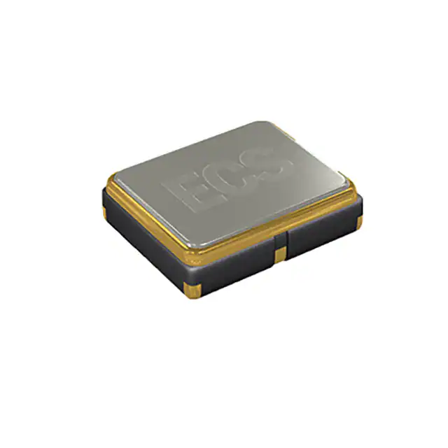
XLH335024.000000I is housed in a 5.0 × 3.2 × 1.2 mm JS6 surface-mount ceramic package (RoHS-compliant, lead-free). This 6-pin SMD oscillator uses standard footprint and reflow profile per JEDEC J-STD-020.
| Pin/Terminal | Circuit Role | Design Meaning |
|---|---|---|
| 1 | E/D (Enable/Disable) | Active-low digital control: logic low disables output (high-impedance); internally pulled high; no external pull-up needed. |
| 2 | NC | No connect - electrically isolated; must remain unconnected per Renesas pin description for XO option. |
| 3 | GND | Signal and power ground reference; tie directly to low-impedance system ground plane. |
| 4 | OUT | LVDS positive output - pair with Pin 5 (OUT2) for true differential signaling; 100 Ω termination required. |
| 5 | OUT2 | LVDS complementary (negative) output - forms differential pair with Pin 4; both pins must be routed length-matched. |
| 6 | VDD | 3.3 V power supply input - bypass with 0.01 µF capacitor to Pin 3 (GND) adjacent to device for noise suppression. |
Key Features
| Feature | Design Value |
|---|---|
| Ultra-low phase jitter | 750 fs typical (12 kHz–20 MHz) - enables clean sampling in high-speed ADCs and low-BER SerDes links. |
| LVDS output compliance | Guaranteed VOD = 0.6 V (3.3 V supply), ODC = 47–53%, tR/tF ≤ 400 ps - ensures interoperability with standard LVDS receivers. |
| Fast enable/disable control | TOE ≤ 100 ns - allows dynamic clock gating in power-sensitive applications without PLL relock delay. |
| Stable frequency accuracy | ±20 ppm over full temp/voltage/load range - eliminates need for system-level calibration in cost-sensitive designs. |
| Short lead-time availability | Standard-frequency XO with no custom programming - shipped from stock or <4-week build cycle per Renesas XO policy. |
Applications
| 10G/25G Ethernet PHY Clocking | FPGA Transceiver Reference |
|---|---|
|
Use Scenario: Providing low-jitter reference clock to SFP28/QSFP28 modules and MAC/PHY ICs in edge routers and switches. IC Role / Device Role / Timing Role: Primary 24 MHz LVDS reference oscillator feeding clock buffer trees and CDR circuits. Use Value: 750 fs phase jitter directly reduces deterministic jitter accumulation in multi-lane SerDes, improving link margin by >2 dB. |
Use Scenario: Supplying clean, stable clock to Xilinx UltraScale+ or Intel Agilex FPGA transceiver banks for PCIe Gen4/5 and 100G KR4 interfaces. IC Role / Device Role / Timing Role: System-level timing source for GTY/GTH/GTP transceivers; synchronized to board-level PLLs. Use Value: ±20 ppm stability over –20°C to +70°C avoids bit slip during thermal cycling; LVDS drive strength supports long trace runs. |
| Industrial PLC Real-Time Controller | Medical Imaging Data Acquisition |
|
Use Scenario: Timing core for ARM Cortex-A9/A53-based motion controllers requiring deterministic I/O response under variable ambient conditions. IC Role / Device Role / Timing Role: Master clock generator for timer peripherals, PWM modules, and EtherCAT slave synchronization. Use Value: 10 ms startup time enables fast boot sequences; robustness to voltage ripple (per IDD specs) ensures reliability in noisy industrial rails. |
Use Scenario: Clocking high-resolution ADCs (≥16-bit, ≥100 MSPS) in ultrasound beamformers and MRI front-ends. IC Role / Device Role / Timing Role: Low-phase-noise sampling clock source; directly drives ADC master clock input with minimal added jitter. Use Value: Sub-1 ps integrated jitter preserves ENOB; LVDS output rejects common-mode noise from switching power supplies near analog sections. |
Equivalent & Alternatives
The following parts are listed as comparable options for similar crystal oscillator applications.
| Alternative Part | Technical Difference | Application Difference | Selection Advice |
|---|---|---|---|
| Si510-24.000000M | CMOS output only; 1.2 ps phase jitter (12 kHz–20 MHz); ±25 ppm stability over –40°C to +85°C. | Lacks LVDS interface; requires external level-shifting for differential receivers; wider temp range but higher jitter. | Select if board already uses CMOS clock distribution and extended temperature operation is mandatory. |
| AK2-24.0000T | LVDS output; 850 fs phase jitter; ±25 ppm stability over –40°C to +85°C; 7.0 × 5.0 mm package. | Same electrical interface but larger footprint; tighter temp range than XLH335024.000000I, yet looser stability spec. | Choose when mechanical space allows larger package and industrial temp range is prioritized over ±20 ppm precision. |
Compared with Si510-24.000000M and AK2-24.0000T, XLH335024.000000I uniquely delivers LVDS output with 750 fs jitter and ±20 ppm stability in a compact 5.0 × 3.2 mm form factor - making it optimal for space-constrained, jitter-critical telecom and FPGA timing applications where commercial-temp operation suffices.
Availability
XLH335024.000000I is available at Aetrix Electronics and suitable for 10G Ethernet PHY clocking, FPGA transceiver reference, industrial PLC timing, and medical imaging data acquisition requiring stable component supply, consistent parametric performance, and RoHS-compliant sourcing.
Supply support for XLH335024.000000I includes scheduled delivery planning, volume procurement assistance, BOM continuity management, traceable sourcing, and lifecycle availability coordination for OEM customers, industrial embedded developers, connected-device designers, and electronics production programs.
Manufacturer
Renesas Electronics Corporation is a global semiconductor leader headquartered in Tokyo, Japan, specializing in microcontrollers, analog, power, and timing solutions for automotive, industrial, and infrastructure markets.
XLH335024.000000I belongs to the XL family of ultra-low-phase-noise quartz-based PLL oscillators, engineered specifically for high-speed serial communication, FPGA/ASIC clocking, and instrumentation systems demanding sub-1 ps jitter and rapid time-to-market.
FAQ
What output type does XLH335024.000000I use, and is it configurable?
XLH335024.000000I uses fixed LVDS output - not software- or pin-configurable. Its pinout (Pins 4/5) and DC/AC specs (VOD ≤ 0.6 V, 100 Ω load) confirm LVDS compliance per Renesas datasheet Tables 9 and 12. No other output types (LVPECL, LVCMOS) are supported for this specific part number.
What is the frequency stability specification for XLH335024.000000I, and what conditions does it cover?
XLH335024.000000I has ±20 ppm frequency stability over –20°C to +70°C, inclusive of initial tolerance, temperature variation, supply voltage change (±5%), load variation, aging, shock, and vibration - as defined in Renesas' "Frequency Stability and Operating Temperature Decoder" table and footnote 2 of the datasheet.
Does XLH335024.000000I support voltage control (VCXO mode)?
No. XLH335024.000000I is an XO (crystal oscillator), not a VCXO. Its ordering code lacks the 'V' suffix used for VCXO variants (e.g., XLHVxxx), and Pin 1 is designated E/D (enable/disable), not Vc. The datasheet explicitly separates XO and VCXO pin assignments and features - XLH335024.000000I matches only the XO configuration.
What is the recommended bypass capacitor for XLH335024.000000I, and where should it be placed?
A 0.01 µF ceramic bypass capacitor must be placed between Pin 6 (VDD) and Pin 3 (GND), as stated in the "Pin Assignments" section of the Renesas XL datasheet. This placement minimizes power supply line noise and ensures stable oscillator operation - a requirement verified across all XL XO variants including XLH335024.000000I.
Is XLH335024.000000I available in smaller packages like 3.2 × 2.5 mm?
No. XLH335024.000000I uses the JS6 (5.0 × 3.2 mm) package. The 3.2 × 2.5 mm (JX6) option is explicitly noted as "not available for VCXO" in the datasheet Features section - and critically, the XLH prefix in the part number maps to the 5.0 × 3.2 mm package per Renesas' Ordering Information (XO) table and Marking Diagrams section.
XLH335024.000000I Specifications
- Product attributes
- Attribute value
- Manufacturer:
- Renesas
- Series:
- XPRESSO™ FXO-HC33
- Package/Case:
- 6-SMD, No Lead
- Packaging:
- Strip
- Product Status:
- Active
- Base Resonator:
- Crystal
- Type:
- XO (Standard)
- Frequency:
- 24 MHz
- Function:
- Enable/Disable
- Output:
- HCMOS
- Voltage - Supply:
- 3.3V
- Frequency Stability:
- ±50ppm
- Absolute Pull Range (APR):
- -
- Operating Temperature:
- -40°C ~ 85°C
- Spread Spectrum Bandwidth:
- -
- Current - Supply (Max):
- 35mA
- Ratings:
- -
- Mounting Type:
- Surface Mount
- Supplier Device Package:
- 4-VDFN (3.2x2.5)
- Size / Dimension:
- 0.130" L x 0.102" W (3.30mm x 2.60mm)
- Height - Seated (Max):
- 0.039" (1.00mm)
XLH335024.000000I FAQ
1.How can I place an order for XLH335024.000000I through Aetrix?
Please submit a Request for Quotation (RFQ) for XLH335024.000000I on Aetrix. Our sales agent will provide a competitive quotation and guide you through the order confirmation once you accept the terms.
2.Are the price and stock information for XLH335024.000000I reliable?
The price and inventory of XLH335024.000000I are updated periodically and may fluctuate due to market conditions. Stock and pricing data are typically refreshed every 24 hours. Quotation validity for XLH335024.000000I is usually 5 days.
3.What payment methods are accepted for XLH335024.000000I?
We accept Wire Transfer, PayPal, Credit Card, Western Union, MoneyGram, and Escrow for XLH335024.000000I transactions.
Note: Certain payment methods may incur a processing fee.
4.How is shipping managed for XLH335024.000000I?
XLH335024.000000I orders can be shipped via leading logistics carriers, including DHL, UPS, FedEx, TNT, or Registered Mail.
Once your XLH335024.000000I order is processed, you will receive an email with the shipment details and tracking number.
Note: Tracking information may take up to 24 hours to appear. Express delivery typically takes 3–5 business days.
5.How can I obtain technical support or documentation for XLH335024.000000I?
For technical support, including XLH335024.000000I datasheets, pinout diagrams, or application guidance, please contact our engineering support team. They can provide detailed documentation and assistance for your XLH335024.000000I requirements.
6.How does Aetrix verify that XLH335024.000000I is sourced from the original manufacturer or authorized distributors?
All XLH335024.000000I products on Aetrix are procured from qualified distributors and authorized channels. Our dedicated quality assurance team conducts strict verification, including traceability checks and, if necessary, third-party testing. This ensures that XLH335024.000000I meets industry standards.
7.What is the process for return or replacement of XLH335024.000000I?
All XLH335024.000000I units undergo pre-shipment inspection (PSI). If there is an issue with XLH335024.000000I, returns or replacements are accepted under the following conditions:
1.Quantity discrepancies, incorrect items, or visible external defects (such as breakage or corrosion), acknowledged by Aetrix.
2.The issue is reported within 90 days of delivery.
3.The XLH335024.000000I part is unused and in its original packaging.
Return procedure for XLH335024.000000I:
1.Submit a request within 90 days.
2.Obtain a Return Material Authorization (RMA) from Aetrix.
XLH335024.000000I Tags
-
ECS-2333-160-BN-TR
ECS Inc.
-
ECS-2333-240-BN-TR
ECS Inc.
-
KC2016Z25.0000C1KX00
KYOCERA AVX
-0.035-Thick.jpg)
-
ECS-2033-250-BN
ECS Inc.
-
O 25,0-JO32-B-1V3-1-T1-LF
Jauch Quartz
-
SIT1533AI-H4-DCC-32.768E
SiTime
-
ECS-2333-500-BN-TR
ECS Inc.
-
COM1305-50.000-EXT-T-TR
Raltron Electronics
-
SG-210STF 24.0000ML0
EPSON
-
ECS-3225MV-320-CN-TR
ECS Inc.
-
ECS-2033-240-BN
ECS Inc.
-
ECS-2333-120-BN-TR
ECS Inc.
Tech Hub

TTL and CMOS logic families differ in thresholds, loading, output drive, power and timing. This engineering guide compares 74HC and 74HCT, calculates noise margins and checks 3.3 V/5 V compatibility.

A practical engineering guide to 3.3V and 5V logic compatibility, input thresholds, resistor dividers, translator ICs, MOSFET level shifting, I2C pull-ups, timing limits and power-sequencing risks.

The 74HC595 uses push-pull logic outputs, while the TPIC6B595 uses 50 V open-drain DMOS sinks for higher-power loads. This guide compares timing, current limits, 3.3 V interfacing, load wiring, thermal…

The 74HC595 converts serial data into eight stable parallel outputs. This guide covers pin functions, shift and storage timing, OE and MR behavior, drive-current limits, cascading, voltage compatibilit…

A technical comparison of level-sensitive latches and edge-triggered flip-flops, covering timing windows, setup and hold limits, master–slave operation, time borrowing, race-through, HDL inference and…

A D latch stores one bit while Enable controls when data can pass. This reference covers gate-level operation, truth tables, transparency, setup and hold timing, LE versus OE, common ICs and practical …

An SR latch stores one bit through cross-coupled feedback. This engineering reference covers NOR and NAND implementations, truth tables, forbidden-state recovery, gated operation, switch debouncing, fa…

Latch circuits retain one bit through feedback. This technical reference covers SR and D latches, truth tables, transparency, timing limits, latch-versus-flip-flop behavior, applications and common log…

An engineering guide to LED driver operation, constant-current and constant-voltage outputs, linear and switching topologies, dimming, IC selection, calculations, replacement compatibility, and fault c…

Operational amplifier guide covering op amp basics, feedback, ideal vs real op amps, common configurations, buffer circuits, offset, bias current, gain-bandwidth, slew rate, rail-to-rail limits and sel…


