
 My Inquiry
 My Account


NXP Semiconductors XPC8240RZU250E
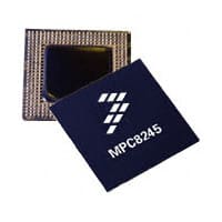
- Part No.:
- XPC8240RZU250E
- Manufacturer:
- NXP Semiconductors
- Category:
- Microprocessors
- Package:
- 352-LBGA
- Datasheet:
-
 XPC8240RZU250E.pdf
- Description:
- IC MPU MPC82XX 250MHZ 352TBGA
- Quantity:
- Payment:

- Shipping:

Inventory:4,515
Please send an inquiry. Send us your inquiry, and we will respond immediately.
Product details
Overview
XPC8240RZU250E from Freescale Semiconductor is a 250 MHz integrated PowerPC processor with MPC603e core, dual PLL architecture (CPU and peripheral/memory bus), 2.625 V ±125 mV core supply, and TBGA package optimized for embedded control applications requiring PCI-to-memory-to-CPU clock domain bridging.
For engineers reviewing the XPC8240RZU250E datasheet, XPC8240RZU250E pinout, XPC8240RZU250E application, or XPC8240RZU250E equivalent, key selection criteria include verified 250 MHz CPU operation under 0–105°C junction temperature, PLL_CFG[0:4]-driven frequency configuration, and compatibility with 33/66 MHz PCI Sync input and 100 MHz memory bus timing.
Technical Context
The XPC8240RZU250E implements two independent PLLs: one for CPU clock generation (memory-to-CPU multiplier up to 4×) and another for peripheral/memory bus clocking (PCI-to-memory multiplier up to 3×), both configurable via PLL_CFG[0:4] pins. It supports PLL bypass mode for hardware modeling and clock-off mode for full power-down.
It operates across 0–105°C die-junction temperature with five dedicated power domains: VDD/AVDD/AVDD2/LAVDD at 2.625 V ±5%, OVDD at 3.3 V ±0.3 V, and GVDD at 3.3 V ±5%. LVDD supports dual 3.3 V or 5.0 V reference with input-tolerant signals on PCI, EPIC control, and OSC_IN.
Key Specifications
| Parameter | Value and Actual Design Meaning |
|---|---|
| CPU Frequency | 250 MHz - guaranteed maximum operating frequency under specified VDD and thermal conditions |
| Core Supply Voltage | 2.625 V ±125 mV DC - nominal VDD/AVDD/AVDD2/LAVDD required for stable 250 MHz operation |
| Junction Temperature | 0 to 105°C - validated thermal operating range for continuous functional operation |
| PCI Sync Input Range | 25–41 MHz - supported PCI_SYNC_IN frequency range for PLL configuration Ref. No. E (01110) |
| Memory Bus Clock | 100 MHz - achievable peripheral logic/memory bus frequency when configured for 250 MHz CPU |
| Power Consumption (Typical) | 3.7 W - measured at 33/100/250 MHz (PCI/Mem/CPU) with cache-resident FP/INT workload |
| Package Type | TBGA - 484-ball thin quad flatpack ball grid array with lead-free (RoHS-compliant) finish |
Pinout & Package
Package: 484-ball TBGA (Thin Ball Grid Array), RoHS-compliant, marked "XPC8240RZU250E" with revision ID 0x13.
| Pin/Terminal | Circuit Role | Design Meaning |
|---|---|---|
| PLL_CFG[0:4] | Configuration input | 5-bit strap setting determining CPU and memory bus PLL multipliers; Ref. No. E = 01110 for 250 MHz operation |
| PCI_SYNC_IN | Input clock reference | Primary PCI bus clock input driving both PLLs; valid range 25–41 MHz for XPC8240RZU250E |
| VDD / AVDD / AVDD2 / LAVDD | Power supply pins | Dedicated 2.625 V supplies for core logic, CPU PLL, peripheral PLL, and DLL respectively |
| OVDD / GVDD | I/O power supplies | 3.3 V supplies for PCI and memory bus drivers; OVDD tolerant to 3.6 V inputs |
| LVDD | PCI reference voltage | Supports 3.3 V or 5.0 V reference; enables input-tolerant signaling on PCI interface and OSC_IN |
Key Features
| Feature | Design Value |
|---|---|
| Dual independent PLLs | Separate CPU VCO (up to 4×) and memory VCO (up to 3×) enable flexible clock domain partitioning |
| Configurable PLL ratios | 19 defined PLL_CFG[0:4] settings including Ref. No. E (01110) optimized for 250 MHz CPU at 100 MHz memory bus |
| Extended thermal range | 0–105°C junction operation validated for industrial and telecom infrastructure environments |
| Input-tolerant I/O | LVDD-referenced signals (PCI, EPIC, OSC_IN) withstand up to 5.75 V input while powered from 3.3 V or 5.0 V |
| Pilot production status | X-prefix denotes limited-volume prototype with preliminary reliability data; requires customer authorization per SOP 3-13 |
Applications
| Industrial Control Gateway | Telecom Line Card |
|---|---|
|
Use Scenario: Real-time protocol translation between legacy fieldbus (Modbus, Profibus) and Ethernet/IP in programmable logic controllers. IC Role / Device Role / Timing Role: Central processing unit managing dual-clock-domain I/O subsystems and PCI-based communication coprocessors. Use Value: 250 MHz CPU performance with deterministic 100 MHz memory bus ensures sub-millisecond response for motion control loops. |
Use Scenario: Channelized T1/E1 aggregation and framing in carrier-grade access equipment. IC Role / Device Role / Timing Role: Host processor interfacing with multiple HDLC or framer ICs via PCI, synchronizing to line-derived clocks. Use Value: LVDD input tolerance allows direct connection to 5 V telecom signaling without level-shifting; 0–105°C operation supports fanless chassis designs. |
| Medical Imaging Subsystem | Ruggedized Data Acquisition |
|
Use Scenario: Image preprocessing pipeline in portable ultrasound systems using FPGA-accelerated filtering and DRAM buffering. IC Role / Device Role / Timing Role: Memory-coherent controller managing SDRAM transfers and PCI-exposed DMA channels to host PC. Use Value: Dual PLL architecture isolates CPU timing from memory bus jitter, preserving ADC sample integrity during burst transfers. |
Use Scenario: High-reliability environmental monitoring in oil/gas downhole tools exposed to extreme temperature cycling. IC Role / Device Role / Timing Role: Embedded controller executing sensor fusion algorithms while maintaining watchdog-managed fault logging over RS-485. Use Value: Verified 0–105°C junction operation eliminates derating concerns; pilot production status permits early integration with qualification planning. |
Equivalent & Alternatives
The following parts are listed as comparable options for similar integrated processor applications.
| Alternative Part | Technical Difference | Application Difference | Selection Advice |
|---|---|---|---|
| MPC8245RZUP250C | Same MPC824x family, 250 MHz, but rated for 0–85°C TJ and uses different PLL_CFG mapping (Ref. No. C = 01100) | Limited to commercial-temperature industrial use; lacks extended thermal validation of XPC8240RZU250E | Select when thermal margin >20°C is available and pilot production constraints are not applicable |
| MPC8240RVV250E | Identical electrical specs and PLL configuration (Ref. No. E), but packaged in 484-pin PBGA instead of TBGA | Requires PCB redesign due to different ball pitch and thermal pad layout; no change in firmware or timing | Choose for legacy PBGA-compatible layouts where board re-spin is feasible |
Compared with MPC8245RZUP250C and MPC8240RVV250E, the XPC8240RZU250E uniquely combines extended 0–105°C operation, TBGA packaging for improved thermal dissipation, and pilot-production readiness for early-system integration-making it optimal for ruggedized, thermally constrained embedded platforms.
Availability
XPC8240RZU250E is available at Aetrix Electronics and suitable for industrial control gateways, telecom line cards, medical imaging subsystems, and ruggedized data acquisition requiring stable component supply through design-in and volume production phases.
Supply support for XPC8240RZU250E includes scheduled delivery planning, volume procurement assistance, BOM continuity management, traceable sourcing, and lifecycle availability coordination for OEM customers, industrial embedded developers, connected-device designers, and electronics production programs.
Manufacturer
Freescale Semiconductor (now part of NXP Semiconductors) was a leading designer of embedded processors, analog, and connectivity solutions for automotive, industrial, and networking markets.
The MPC8240 product line delivers integrated PowerPC-based system-on-chip solutions targeting PCI-based embedded control applications with tight thermal and power constraints.
FAQ
What does the "X" prefix in XPC8240RZU250E signify?
The "X" prefix in XPC8240RZU250E indicates a pilot production prototype per Freescale SOP 3-13: a limited-volume run manufactured and tested on qualified technology with preliminary reliability data. Customers must provide written authorization before deployment, acknowledging potential for product changes during shipment.
What PLL configuration is required to achieve 250 MHz CPU operation on XPC8240RZU250E?
XPC8240RZU250E achieves 250 MHz CPU operation using PLL_CFG[0:4] = 01110 (Ref. No. E), which configures the memory bus at 100 MHz and applies a 2.5× CPU VCO multiplier to a 100 MHz memory clock. This setting is validated for 25–41 MHz PCI_SYNC_IN input.
Is XPC8240RZU250E compatible with standard 3.3 V PCI signaling?
Yes, XPC8240RZU250E supports standard 3.3 V PCI signaling via its OVDD supply (3.3 V ±0.3 V) and LVDD-referenced input-tolerant pins. The PCI interface signals tolerate up to 3.6 V input when LVDD is set to 3.3 V, meeting PCI Local Bus Specification 2.2 requirements.
How does the power consumption of XPC8240RZU250E compare across operating modes?
XPC8240RZU250E draws 3.7 W typical at 33/100/250 MHz (PCI/Mem/CPU), drops to 2.6 W in Doze mode, 900 mW in Nap mode, and 500–800 mW in Sleep mode depending on clock enable states-enabling dynamic power management in thermally constrained systems.
What package and marking details identify XPC8240RZU250E?
XPC8240RZU250E uses a 484-ball TBGA package with lead-free finish. Marking includes "XPC8240RZU250E", 6-digit mask number (MMMMMM), and traceability code (ATWLYYWWA); revision ID 0x13 is readable from address offset 0x08.
XPC8240RZU250E Specifications
- Product attributes
- Attribute value
- Manufacturer:
- NXP Semiconductors
- Package/Case:
- 352-LBGA
- Series:
- MPC82xx
- Packaging:
- Tray
- Product Status:
- Obsolete
- Core Processor:
- PowerPC 603e
- Number of Cores/Bus Width:
- 1 Core, 32-Bit
- Speed:
- 250MHz
- Co-Processors/DSP:
- -
- RAM Controllers:
- DRAM, SDRAM
- Graphics Acceleration:
- No
- Display & Interface Controllers:
- -
- Ethernet:
- -
- SATA:
- -
- USB:
- -
- Voltage - I/O:
- 3.3V
- Operating Temperature:
- 0°C ~ 105°C (TA)
- Grade:
- -
- Qualification:
- -
- Security Features:
- -
- Mounting Type:
- Surface Mount
- Supplier Device Package:
- 352-TBGA (35x35)
- Additional Interfaces:
- I2C, I²O, PCI, UART
XPC8240RZU250E FAQ
1.How can I place an order for XPC8240RZU250E through Aetrix?
Please submit a Request for Quotation (RFQ) for XPC8240RZU250E on Aetrix. Our sales agent will provide a competitive quotation and guide you through the order confirmation once you accept the terms.
2.Are the price and stock information for XPC8240RZU250E reliable?
The price and inventory of XPC8240RZU250E are updated periodically and may fluctuate due to market conditions. Stock and pricing data are typically refreshed every 24 hours. Quotation validity for XPC8240RZU250E is usually 5 days.
3.What payment methods are accepted for XPC8240RZU250E?
We accept Wire Transfer, PayPal, Credit Card, Western Union, MoneyGram, and Escrow for XPC8240RZU250E transactions.
Note: Certain payment methods may incur a processing fee.
4.How is shipping managed for XPC8240RZU250E?
XPC8240RZU250E orders can be shipped via leading logistics carriers, including DHL, UPS, FedEx, TNT, or Registered Mail.
Once your XPC8240RZU250E order is processed, you will receive an email with the shipment details and tracking number.
Note: Tracking information may take up to 24 hours to appear. Express delivery typically takes 3–5 business days.
5.How can I obtain technical support or documentation for XPC8240RZU250E?
For technical support, including XPC8240RZU250E datasheets, pinout diagrams, or application guidance, please contact our engineering support team. They can provide detailed documentation and assistance for your XPC8240RZU250E requirements.
6.How does Aetrix verify that XPC8240RZU250E is sourced from the original manufacturer or authorized distributors?
All XPC8240RZU250E products on Aetrix are procured from qualified distributors and authorized channels. Our dedicated quality assurance team conducts strict verification, including traceability checks and, if necessary, third-party testing. This ensures that XPC8240RZU250E meets industry standards.
7.What is the process for return or replacement of XPC8240RZU250E?
All XPC8240RZU250E units undergo pre-shipment inspection (PSI). If there is an issue with XPC8240RZU250E, returns or replacements are accepted under the following conditions:
1.Quantity discrepancies, incorrect items, or visible external defects (such as breakage or corrosion), acknowledged by Aetrix.
2.The issue is reported within 90 days of delivery.
3.The XPC8240RZU250E part is unused and in its original packaging.
Return procedure for XPC8240RZU250E:
1.Submit a request within 90 days.
2.Obtain a Return Material Authorization (RMA) from Aetrix.
XPC8240RZU250E Tags

-
AT91SAM9260B-CU-999
Microchip Technology
-
AT91SAM9G25-CU
Microchip Technology

-
ATSAMA5D27C-CU
Microchip Technology
-
AT91SAM9X35-CU
Microchip Technology
-
AT91SAM9X25-CU
Microchip Technology

-
MCIMX6Y2CVM08AB
NXP Semiconductors
.JPG)
-
AM3352BZCZ100
Texas Instruments
-
AT91SAM9260B-CU
Microchip Technology

-
AT91SAM9260B-QU
Microchip Technology

-
ATSAMA5D31A-CU
Microchip Technology
-
AT91SAM9G20B-CU-999
Microchip Technology
-
MCIMX6Y2CVM05AB
NXP Semiconductors
Tech Hub

A practical engineering guide to 3.3V and 5V logic compatibility, input thresholds, resistor dividers, translator ICs, MOSFET level shifting, I2C pull-ups, timing limits and power-sequencing risks.

The 74HC595 uses push-pull logic outputs, while the TPIC6B595 uses 50 V open-drain DMOS sinks for higher-power loads. This guide compares timing, current limits, 3.3 V interfacing, load wiring, thermal…

The 74HC595 converts serial data into eight stable parallel outputs. This guide covers pin functions, shift and storage timing, OE and MR behavior, drive-current limits, cascading, voltage compatibilit…

A technical comparison of level-sensitive latches and edge-triggered flip-flops, covering timing windows, setup and hold limits, master–slave operation, time borrowing, race-through, HDL inference and…

A D latch stores one bit while Enable controls when data can pass. This reference covers gate-level operation, truth tables, transparency, setup and hold timing, LE versus OE, common ICs and practical …

An SR latch stores one bit through cross-coupled feedback. This engineering reference covers NOR and NAND implementations, truth tables, forbidden-state recovery, gated operation, switch debouncing, fa…

Latch circuits retain one bit through feedback. This technical reference covers SR and D latches, truth tables, transparency, timing limits, latch-versus-flip-flop behavior, applications and common log…

An engineering guide to LED driver operation, constant-current and constant-voltage outputs, linear and switching topologies, dimming, IC selection, calculations, replacement compatibility, and fault c…

Operational amplifier guide covering op amp basics, feedback, ideal vs real op amps, common configurations, buffer circuits, offset, bias current, gain-bandwidth, slew rate, rail-to-rail limits and sel…

Jumper cables guide covering safe connection order, red and black clamp placement, final ground connection, cable gauge, length, clamp quality, copper vs CCA cables, jump starter comparison and battery…


