
 My Inquiry
 My Account


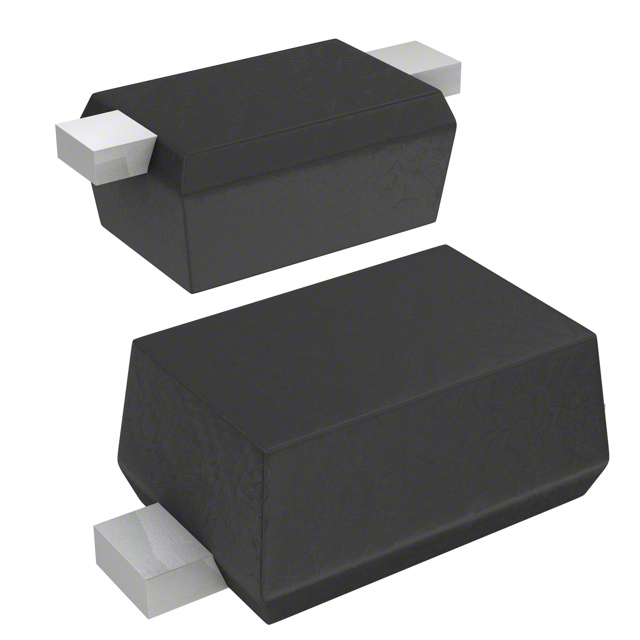
Diodes Incorporated ZC833BTA
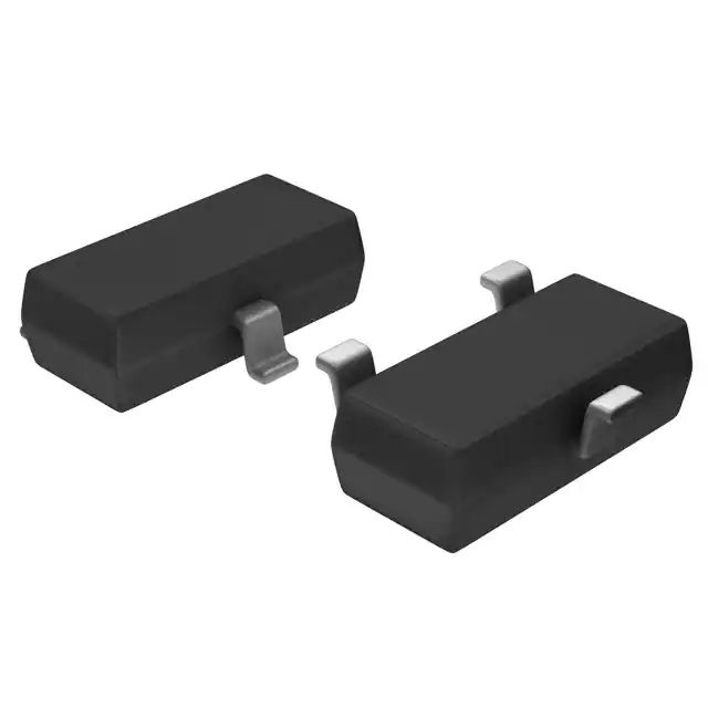
- Part No.:
- ZC833BTA
- Manufacturer:
- Diodes Incorporated
- Package:
- TO-236-3, SC-59, SOT-23-3
- Datasheet:
-
 ZC833BTA.pdf
- Description:
- DIODE VARACTOR CAP SOT23-3
- Quantity:
- Payment:

- Shipping:

Inventory:6,590
Please send an inquiry. Send us your inquiry, and we will respond immediately.
Product details
Overview
ZC833BTA from Zetex Semiconductors is a silicon hyperabrupt varactor diode optimized for voltage-controlled frequency tuning in precision oscillators and RF filters. It delivers 33.0 pF nominal capacitance at 2 V, 5.0–6.5 capacitance ratio (C₂/C₂₀), ≥200 Q at 50 MHz/3 V, and ultra-low reverse leakage (typ. 200 pA), enabling low-phase-noise VCXO/TCXO designs in wireless infrastructure.
For engineers reviewing the ZC833BTA datasheet, ZC833BTA pinout, ZC833BTA application, or ZC833BTA equivalent, key selection criteria include its SOT23 package compatibility, hyperabrupt CV slope for steep tuning response, guaranteed C₂/C₂₀ ≥5.0, and operation up to +150°C ambient - critical for stable RF front-end and timing module design.
Technical Context
The ZC833BTA is a single-die, cathode-marked hyperabrupt junction varactor with tightly controlled doping profile to achieve steep, linearized C–V response across 2–20 V. Its 33.0 pF nominal capacitance at 2 V and 5.0–6.5 C₂/C₂₀ ratio are specified at 1 MHz, supporting wide-range frequency pulling in oscillator tanks.
Designed for RF signal path tuning, it operates with ≤20 nA reverse leakage at 20 V and exhibits a temperature coefficient of capacitance of +300 to +400 ppm/°C - a known trade-off for hyperabrupt devices that must be compensated in TCXO loop design.
Key Specifications
| Parameter | Value and Actual Design Meaning |
|---|---|
| Capacitance @ 2 V | 31.35–34.65 pF - defines baseline tank impedance and sets oscillator center frequency range |
| C₂/C₂₀ Ratio | ≥5.0 - enables ≥5× frequency tuning range without significant distortion or nonlinearity |
| Q Factor @ 50 MHz | ≥200 - minimizes insertion loss and phase noise degradation in resonant circuits |
| Reverse Leakage @ 20 V | ≤20 nA - ensures low DC bias current draw and stable tuning voltage in low-power VCXOs |
| Max Reverse Voltage | 25 V - supports wide tuning voltage swing while maintaining junction integrity |
| Operating Temp Range | −55°C to +150°C - qualified for automotive under-hood and industrial base station environments |
Pinout & Package
Package: SOT23 - surface-mount, 3-lead plastic package with cathode-indicating marking (J2B), 2.67–3.05 mm length, 1.20–1.40 mm width, 0.95 mm nominal height.
| Pin/Terminal | Circuit Role | Design Meaning |
|---|---|---|
| Anode (Pin 1) | DC tuning voltage input | Accepts 0–20 V control voltage; reverse-biased during operation |
| Cathode (Pin 2) | RF ground reference | Connected to RF ground plane; serves as common node for tank circuit return |
| No-connect (Pin 3) | Thermal pad / mechanical anchor | Internally tied to cathode in ZC833BTA; enhances thermal dissipation and solder joint reliability |
Key Features
| Feature | Design Value |
|---|---|
| Hyperabrupt junction profile | Engineered doping gradient delivers steeper dC/dV than abrupt junctions - essential for wide, linear frequency sweep |
| Closely controlled CV tolerance | ±1.5% capacitance spread at 2 V - reduces binning needs and improves oscillator yield across production lots |
| Low IR (200 pA typ.) | Minimizes tuning voltage droop and drift in high-impedance bias networks - critical for low-phase-noise VCXOs |
| High Q ≥200 @ 50 MHz | Reduces resonator losses by >3 dB vs. standard varactors - directly improves oscillator close-in phase noise floor |
Applications
| VCXO Frequency Tuning | TCXO Compensation Network |
|---|---|
Use Scenario: Fine-tuning of 10–100 MHz crystal oscillator output in telecom clock modules. IC Role / Device Role / Timing Role: Voltage-variable capacitor in Colpitts tank, adjusting resonant frequency via analog control voltage. Use Value: Enables ±50 ppm pull range with <−140 dBc/Hz phase noise at 1 kHz offset due to low IR and high Q. | Use Scenario: Temperature-compensated frequency adjustment in GPS receiver reference oscillators. IC Role / Device Role / Timing Role: Varactor paired with thermistor network to counteract crystal's parabolic frequency vs. temperature curve. Use Value: Tight CV matching (±1.5%) ensures consistent compensation slope across batches, reducing calibration overhead. |
| RF Bandpass Filter Tuning | Wireless Transceiver VCO Core |
Use Scenario: Channel-select bandpass filter in 802.11a/n front-end with 5 GHz tuning range. IC Role / Device Role / Timing Role: Tuning element in parallel-resonant LC section; adjusted dynamically for channel hopping. Use Value: C₂/C₂₀ ≥5.0 supports full 5 GHz band coverage with single filter topology - eliminating need for switched banks. | Use Scenario: Core tuning diode in 2.4 GHz ISM-band VCO for Bluetooth LE transceivers. IC Role / Device Role / Timing Role: Primary varactor in negative-Gm LC oscillator core, biased at 3 V for optimal Q and linearity. Use Value: SOT23 footprint and 33 pF nominal value match standard 2.4 GHz tank design rules - enabling drop-in layout reuse. |
Equivalent & Alternatives
The following parts are listed as comparable options for similar varactor diode applications.
| Alternative Part | Technical Difference | Application Difference | Selection Advice |
|---|---|---|---|
| SMV2023-011LF | Higher C₂/C₂₀ (7.0), lower C₀ (22 pF @ 2 V), SOD-323 package | Better for narrowband VCOs needing higher tuning ratio but less capacitance headroom | Select when tuning range >6× required and board space allows smaller SOD-323 footprint |
| BBY52-02W | Lower Q (150 @ 50 MHz), wider C tolerance (±10%), same SOT23 package | Suitable for cost-sensitive consumer radios where phase noise is secondary | Choose for non-critical filtering where leakage <100 nA suffices and BOM cost is prioritized |
Compared with SMV2023-011LF and BBY52-02W, ZC833BTA offers superior Q and tighter CV matching - making it preferred for low-phase-noise VCXOs and production-grade TCXOs where stability and repeatability are mandatory.
Availability
ZC833BTA is available at Aetrix Electronics and suitable for VCXO design, TCXO manufacturing, and RF filter tuning requiring stable component supply, tight parametric consistency, and RoHS-compliant SMT assembly.
Supply support for ZC833BTA includes scheduled delivery planning, volume procurement assistance, BOM continuity management, traceable sourcing, and lifecycle availability coordination for OEM customers, industrial embedded developers, connected-device designers, and electronics production programs.
Manufacturer
Zetex Semiconductors plc was a UK-based ISO 9001/TS16949-certified designer and manufacturer of high-performance analog and RF semiconductors, acquired by Diodes Incorporated in 2008.
The 830 series varactors were developed specifically for precision frequency control in wireless infrastructure and timing modules - emphasizing hyperabrupt CV linearity, low leakage, and high-Q RF performance in miniature packages.
FAQ
What is the maximum recommended reverse voltage for continuous operation?
The absolute maximum reverse voltage is 25 V per the datasheet, but sustained operation above 20 V increases risk of accelerated junction degradation. For reliable long-term use in VCXOs, Zetex specifies derated operation at ≤20 V with IR ≤20 nA - ensuring stable capacitance and minimal phase noise drift over 10+ years.
Does ZC833BTA have a built-in ESD protection structure?
No - ZC833BTA lacks integrated ESD protection. Its junction is rated for ≤250 V HBM per Zetex's internal qualification, so PCB-level protection (e.g., series resistor + shunt TVS) is required in handling and system integration. ESD damage typically manifests as increased IR or reduced C₂/C₂₀ before catastrophic failure.
Can ZC833BTA be used in dual-common-cathode configuration?
No - ZC833BTA is a single-diode variant in SOT23. Dual configurations (e.g., ZDC833) use SOT-23-6 or SOT-363 packages with separate anodes and shared cathode. Attempting dual use with ZC833BTA would require external parallel connection, degrading Q and introducing parasitic coupling.
How does temperature affect capacitance tuning linearity?
Capacitance shifts +300 to +400 ppm/°C, causing ~0.5% C change over −40°C to +85°C. This introduces curvature in C–V slope versus temperature - requiring either analog compensation (thermistor network) or digital lookup-table correction in closed-loop TCXOs to maintain frequency accuracy within ±0.1 ppm.
ZC833BTA Specifications
- Product attributes
- Attribute value
- Manufacturer:
- Diodes Incorporated
- Series:
- -
- Package/Case:
- TO-236-3, SC-59, SOT-23-3
- Packaging:
- Tape & Reel (TR)
- Product Status:
- Obsolete
- Capacitance @ Vr, F:
- 34.65pF @ 2V, 1MHz
- Capacitance Ratio:
- 6.5
- Capacitance Ratio Condition:
- C2/C20
- Voltage - Peak Reverse (Max):
- 25 V
- Diode Type:
- Single
- Q @ Vr, F:
- 200 @ 3V, 50MHz
- Operating Temperature:
- -55°C ~ 150°C (TJ)
- Grade:
- -
- Qualification:
- -
- Mounting Type:
- Surface Mount
- Supplier Device Package:
- SOT-23-3
ZC833BTA FAQ
1.How can I place an order for ZC833BTA through Aetrix?
Please submit a Request for Quotation (RFQ) for ZC833BTA on Aetrix. Our sales agent will provide a competitive quotation and guide you through the order confirmation once you accept the terms.
2.Are the price and stock information for ZC833BTA reliable?
The price and inventory of ZC833BTA are updated periodically and may fluctuate due to market conditions. Stock and pricing data are typically refreshed every 24 hours. Quotation validity for ZC833BTA is usually 5 days.
3.What payment methods are accepted for ZC833BTA?
We accept Wire Transfer, PayPal, Credit Card, Western Union, MoneyGram, and Escrow for ZC833BTA transactions.
Note: Certain payment methods may incur a processing fee.
4.How is shipping managed for ZC833BTA?
ZC833BTA orders can be shipped via leading logistics carriers, including DHL, UPS, FedEx, TNT, or Registered Mail.
Once your ZC833BTA order is processed, you will receive an email with the shipment details and tracking number.
Note: Tracking information may take up to 24 hours to appear. Express delivery typically takes 3–5 business days.
5.How can I obtain technical support or documentation for ZC833BTA?
For technical support, including ZC833BTA datasheets, pinout diagrams, or application guidance, please contact our engineering support team. They can provide detailed documentation and assistance for your ZC833BTA requirements.
6.How does Aetrix verify that ZC833BTA is sourced from the original manufacturer or authorized distributors?
All ZC833BTA products on Aetrix are procured from qualified distributors and authorized channels. Our dedicated quality assurance team conducts strict verification, including traceability checks and, if necessary, third-party testing. This ensures that ZC833BTA meets industry standards.
7.What is the process for return or replacement of ZC833BTA?
All ZC833BTA units undergo pre-shipment inspection (PSI). If there is an issue with ZC833BTA, returns or replacements are accepted under the following conditions:
1.Quantity discrepancies, incorrect items, or visible external defects (such as breakage or corrosion), acknowledged by Aetrix.
2.The issue is reported within 90 days of delivery.
3.The ZC833BTA part is unused and in its original packaging.
Return procedure for ZC833BTA:
1.Submit a request within 90 days.
2.Obtain a Return Material Authorization (RMA) from Aetrix.
ZC833BTA Tags
-
BBY5702VH6327XTSA1
Infineon Technologies
-
BBY5602VH6327XTSA1
Infineon Technologies
-
SMV1405-040LF
Skyworks Solutions Inc.
-
BBY6502VH6327XTSA1
Infineon Technologies
-
BBY6602VH6327XTSA1
Infineon Technologies
-
BBY5802VH6327XTSA1
Infineon Technologies
.jpg)
-
BB175X
NXP USA Inc.
-
SMV1430-040LF
Skyworks Solutions Inc.
-
SMV1273-079LF
Skyworks Solutions Inc.
-
SMV1255-079LF
Skyworks Solutions Inc.
-
SMV1213-079LF
Skyworks Solutions Inc.
-
SMV1247-079LF
Skyworks Solutions Inc.
Tech Hub

An engineering guide to LED driver operation, constant-current and constant-voltage outputs, linear and switching topologies, dimming, IC selection, calculations, replacement compatibility, and fault c…

Operational amplifier guide covering op amp basics, feedback, ideal vs real op amps, common configurations, buffer circuits, offset, bias current, gain-bandwidth, slew rate, rail-to-rail limits and sel…

Jumper cables guide covering safe connection order, red and black clamp placement, final ground connection, cable gauge, length, clamp quality, copper vs CCA cables, jump starter comparison and battery…

LDO regulator guide covering low dropout voltage, power dissipation, thermal design, PSRR, output noise, capacitor stability, adjustable LDO circuits, LDO vs buck converter and datasheet selection chec…

Conditional Access Module guide covering CAM meaning, CI/CI+ interface, smart card authorization, DVB security workflow, TV and set-top box compatibility, internal electronics, ESD protection, connecto…

Guide to electronic component obsolescence covering EOL risk, PCN/PDN notices, last-time buy planning, replacement options, form-fit-function validation, counterfeit risk and BOM lifecycle management.

18650 battery guide covering lithium-ion cell basics, 3.6V/3.7V voltage, 4.2V charging, mAh and Wh capacity, protected cells, chargers, BMS, series-parallel packs, holders, welding and sourcing checks.…

Hall effect sensor guide covering working principle, linear and digital sensors, Arduino circuits, current sensing, speed detection, automotive applications, A3144 examples, signal filtering and datash…

Product Change Notification guide for electronic components, covering PCN meaning, PCN vs PDN/EOL, common change types, risk levels, form-fit-function review, engineering validation, BOM control, LTB/L…

A practical guide to blend door actuators, covering HVAC function, symptoms, location, AC and heater issues, reset and calibration, replacement cost, electrical diagnosis, compatibility checks, and rep…


