
 My Inquiry
 My Account


Renesas ZSSC3240CC5B

- Part No.:
- ZSSC3240CC5B
- Manufacturer:
- Renesas
- Category:
- Sensor and Detector Interfaces
- Package:
- Die
- Datasheet:
-
 ZSSC3240CC5B.pdf
- Description:
- IC SENSOR SIGNAL CONDITIONER
- Quantity:
- Payment:

- Shipping:

Inventory:4,276
Please send an inquiry. Send us your inquiry, and we will respond immediately.
Product details
Overview
ZSSC3240CC5B from Renesas Electronics is a sensor signal conditioning IC (SSC) for resistive sensors, featuring 24-bit ADC resolution, 16-bit DAC output, programmable PGA gain (1.32–540 V/V), on-chip temperature sensing, and I²C/SPI/OWI digital interfaces. It supports bridge, half-bridge, Pt100, and external diode sensors in industrial pressure, flow, and medical blood pressure monitoring systems.
For engineers reviewing the ZSSC3240CC5B datasheet, ZSSC3240CC5B pinout, ZSSC3240CC5B application, or ZSSC3240CC5B equivalent, this page delivers verified technical context, real-world analog/digital output configurations, measurement scheduler behavior, diagnostic coverage, and calibrated smart-sensor design constraints - all specific to the 24-QFN packaged ZSSC3240CC5B variant.
Technical Context
The ZSSC3240CC5B implements a dual-stage programmable-gain amplifier (PGA) with 120 gain steps and ±2.5% gain error, feeding a 12–24-bit ADC with ENOB up to 18.1 bits. Its 26-bit math core executes sensor-specific correction algorithms using coefficients stored in reprogrammable NVM.
It supports three operational modes: wake-up-on-request, continuous/fast-response, and automatic cyclic measurement - each configurable via the measurement scheduler to balance update rate (up to 2.91 kHz), energy consumption (as low as 1.5 µA idle), accuracy, and self-diagnostic coverage including sensor connection, chipping check, and memory integrity verification.
Key Specifications
| Parameter | Value and Actual Design Meaning |
|---|---|
| ADC Resolution | 12–24-bit selectable; enables trade-off between noise floor (24-bit) and conversion speed (13 kHz at 12-bit). |
| DAC Resolution | 13–16-bit programmable; supports precise 0–1 V, 0–5 V, ratiometric, or 4–20 mA analog outputs. |
| PGA Gain Range | 1.32–540 V/V in 120 steps; accommodates sensor spans from 1 mV/V to 500 mV/V without external amplification. |
| Supply Voltage | 2.7–5.5 V (IC); extends to 48 V with external JFET via LDOctrl pin - critical for industrial current-loop designs. |
| Operating Temp | −40°C to +125°C; qualified for under-hood automotive, factory automation, and medical monitoring environments. |
| Sensor Resistance | 0.5 kΩ to 60 kΩ; covers Pt100 RTDs, strain gauges, and NTC/PTC thermistors in single- or bridge-element configurations. |
| Digital Interfaces | I²C (up to 3.4 Mbps), SPI (up to 10 MHz), OWI (100 kbps); allows flexible host integration with minimal pin count. |
Pinout & Package
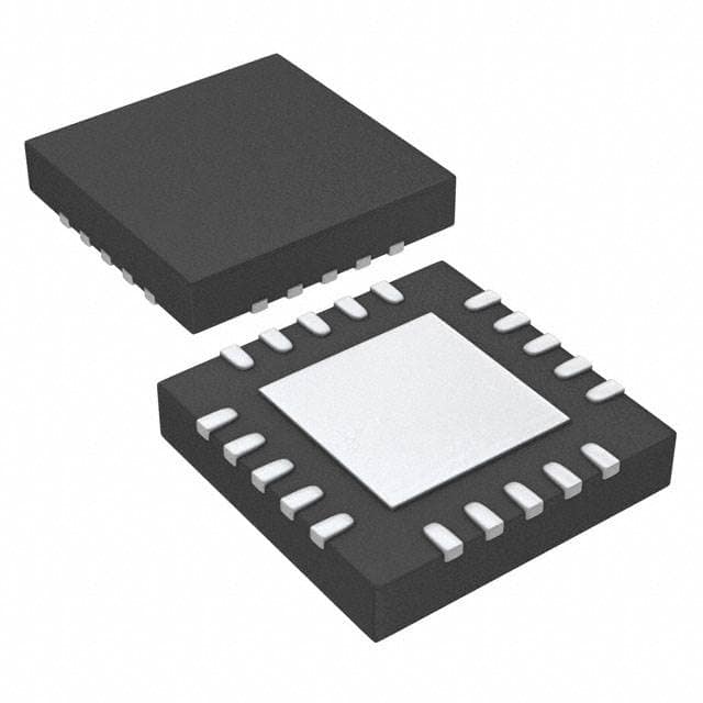
Package: 4 × 4 mm² 24-pin QFN with wettable flanks (exposed thermal pad). Pinout validated per Renesas ZSSC3240 datasheet Rev. Dec.10.24, Page 6–7.
| Pin/Terminal | Circuit Role | Design Meaning |
|---|---|---|
| INP / INN | Differential analog input | Accepts bridge/half-bridge sensor signals; supports common-mode range of 0.7–1.0 V with internal VDDB regulation. |
| VDDB / VSSB | Sensor supply rails | Provides ratiometric or current-mode bias to sensor elements; VDDB internally regulated at 1.68–1.80 V. |
| AOUT / OWI1 | Multi-function terminal | Delivers analog output (voltage/current) or serves as OWI bidirectional data line; includes short-circuit protection (10–12 mA). |
| LDOctrl | Analog control output | Drives external transistor (e.g., JFET) to regulate VDD up to 48 V - essential for high-voltage current-loop applications. |
| EOC | Digital interrupt output | Signals end-of-conversion or threshold-triggered event; enables low-power polling or hardware-driven system response. |
| MOSI/SDA, MISO, SCLK/SCL, SS | Digital interface I/O | Supports concurrent SPI/I²C operation; SCLK/SCL referenced to VDD level; internal pull-ups on MOSI/SDA and SS. |
Key Features
| Feature | Design Value |
|---|---|
| 26-bit sensor math core | Executes full offset, sensitivity, temperature drift, and non-linearity correction using NVM-stored coefficients - eliminates need for external microcontroller compensation. |
| Programmable measurement scheduler | Enables deterministic cyclic sensing with user-defined trade-offs among update rate (0.07–2.91 kHz), power (down to 1.5 µA idle), and diagnostic depth. |
| On-chip diagnostics | Verifies sensor connection integrity, chip chipping status, and NVM memory health - meets functional safety requirements for industrial and medical use. |
| Triple analog output modes | Configurable 0–1 V / 0–5 V absolute, VDD-ratiometric (2.5–97.5%), or 4–20 mA current loop - simplifies interface to PLCs, DAQs, and analog inputs. |
| External temperature sensing | Supports Pt100, external diodes, or bridge-as-temperature-detector via TEXT pin with built-in 150 Ω series resistor for ESD protection. |
Applications
| Industrial Pressure Sensing | Medical Blood Pressure Monitoring |
|---|---|
|
Use Scenario: High-accuracy differential pressure measurement in HVAC ducts and process control valves using silicon piezoresistive bridges. IC Role / Device Role / Timing Role: Signal conditioner performing real-time 24-bit digitization, temperature-compensated linearization, and ratiometric voltage output synchronized to cyclic scheduler. Use Value: Achieves ≤0.01% FSO total error over −40°C to 125°C without external calibration hardware or firmware. |
Use Scenario: Portable sphygmomanometer requiring low-power, high-precision analog output compatible with clinical-grade ADC front-ends. IC Role / Device Role / Timing Role: Smart sensor hub delivering 16-bit corrected digital results via I²C and 0–5 V analog output with <150 µs DAC settling time. Use Value: Enables battery life >1 year via 1.5 µA idle current and wake-on-event operation while maintaining medical-grade accuracy. |
| Factory Automation Flow Meters | White Goods Level Sensing |
|
Use Scenario: Coriolis or turbine-based flow transmitters needing robust 4–20 mA loop output with diagnostics for predictive maintenance. IC Role / Device Role / Timing Role: Current-loop driver with integrated diagnostics (sensor disconnect, memory fault) and LDOctrl-controlled 24 V regulation. Use Value: Eliminates discrete current-source IC and external watchdog, reducing BOM count by 3 components and enabling HART-compatible smart transmitters. |
Use Scenario: Washing machine drum-level detection using resistive string sensors exposed to moisture and vibration. IC Role / Device Role / Timing Role: Ruggedized conditioner with chipping-check diagnostics, wettable-flank QFN package, and EMC-optimized AOUT filtering (22 nF recommended). Use Value: Survives 1000+ thermal cycles and passes IEC 61000-4-2/4-4 compliance with no layout redesign beyond CAOUT,EMC capacitor placement. |
Equivalent & Alternatives
The following parts are listed as comparable options for similar sensor signal conditioning applications.
| Alternative Part | Technical Difference | Application Difference | Selection Advice |
|---|---|---|---|
| TDK InvenSense ICM-20948 | IMU with integrated 9-axis motion sensing; lacks dedicated resistive sensor front-end, PGA, or NVM-based correction math core. | Targets inertial sensing only; not suitable for bridge/Pt100 conditioning or analog output generation. | Select ZSSC3240CC5B when conditioning resistive elements with embedded correction - not for motion fusion or gyro/accelerometer use. |
| Analog Devices AD7798 | 24-bit ΣΔ ADC with PGA and reference; no integrated DAC, NVM, diagnostics, or multi-interface support - requires external MCU for correction. | Requires separate microcontroller, EEPROM, and analog output circuitry to match ZSSC3240CC5B's smart-sensor functionality. | Choose ZSSC3240CC5B for turnkey smart sensor modules; AD7798 suits custom designs where full control over algorithm and interface is needed. |
Compared with ICM-20948 and AD7798, the ZSSC3240CC5B uniquely integrates sensor-specific correction math, reprogrammable NVM, triple-output analog capability, and production-ready diagnostics - reducing system-level component count, firmware development, and qualification effort for calibrated resistive sensor applications.
Availability
ZSSC3240CC5B is available at Aetrix Electronics and suitable for industrial pressure transmitters, medical blood pressure monitors, factory automation flow meters, and white goods level sensors requiring stable component supply across extended temperature ranges and long product lifecycles.
Supply support for ZSSC3240CC5B includes scheduled delivery planning, volume procurement assistance, BOM continuity management, traceable sourcing, and lifecycle availability coordination for OEM customers, industrial embedded developers, connected-device designers, and electronics production programs.
Manufacturer
Renesas Electronics is a global semiconductor leader specializing in microcontrollers, analog, power, and sensor solutions for industrial, automotive, and IoT markets.
The ZSSC3240CC5B belongs to Renesas' Sensor Signal Conditioner product line, designed specifically to enable high-accuracy, low-power, and functionally safe smart sensors for harsh-environment industrial and medical applications.
FAQ
What sensor types does the ZSSC3240CC5B support?
The ZSSC3240CC5B supports resistive bridge and half-bridge sensors, Pt100 RTDs, NTC/PTC thermistors, and external temperature diodes. It accommodates sensor resistances from 0.5 kΩ to 60 kΩ and signal spans from 1 mV/V to 500 mV/V. The device provides both ratiometric and current-mode biasing via VDDB/VSSB and TEXT pins, with built-in 150 Ω series resistance for diode protection - all confirmed in the ZSSC3240CC5B datasheet Section 6.2.4.
How does the ZSSC3240CC5B handle temperature compensation?
The ZSSC3240CC5B performs full digital temperature compensation using its 26-bit math core and NVM-stored coefficients. It corrects offset, sensitivity drift, and non-linearity across −40°C to +125°C. Compensation leverages either the on-chip temperature sensor or external sources (e.g., bridge-as-temperature-detector, Pt100, or diode via TEXT pin). This is implemented without external software - the ZSSC3240CC5B delivers fully corrected S/T digital outputs or analog outputs directly.
Can the ZSSC3240CC5B generate a 4–20 mA current loop output?
Yes, the ZSSC3240CC5B supports 4–20 mA current-loop output using its AOUT/OWI1 pin in conjunction with the FB pin and an external bipolar transistor. The LDOctrl pin enables regulation of higher supply voltages (up to 48 V) required for compliant loop operation. Configuration is programmable via NVM settings, and the ZSSC3240CC5B includes diagnostics for loop integrity - details are specified in Section 6.5.3.3 and Figure 21 of the ZSSC3240CC5B datasheet.
What are the power consumption characteristics of the ZSSC3240CC5B?
The ZSSC3240CC5B draws 1.5–6 µA in idle state (depending on temperature), 2.3–2.8 mA during active operation, and as low as 3.5 µA average per second in cyclic 16-bit digital-only mode. Its measurement scheduler allows fine-grained control over update rate vs. current draw - achieving 0.07–2.91 kHz output rates while maintaining sub-µA sleep currents. These values are measured per Table 4 in the ZSSC3240CC5B datasheet under defined operating conditions.
Does the ZSSC3240CC5B include built-in diagnostics?
Yes, the ZSSC3240CC5B integrates on-chip diagnostics covering sensor connection status, broken-chip (chipping) detection, and NVM memory integrity. Diagnostic results are accessible via the CHECK_DIAG command and reported in the diagnostic register (diagnosticreg[15:0]). These features support functional safety requirements in industrial and medical applications - confirmed in Sections 6.3 and Table 16 of the ZSSC3240CC5B datasheet.
ZSSC3240CC5B Specifications
- Product attributes
- Attribute value
- Manufacturer:
- Renesas
- Package/Case:
- Die
- Series:
- -
- Packaging:
- Bulk
- Product Status:
- Active
- Programmable:
- Not Verified
- Type:
- Resistive
- Input Type:
- Analog
- Output Type:
- 1-Wire®, I2C, SPI
- Current - Supply:
- 2.8 mA
- Operating Temperature:
- -40°C ~ 85°C (TA)
- Grade:
- -
- Qualification:
- -
- Mounting Type:
- Surface Mount
- Supplier Device Package:
- Die
ZSSC3240CC5B FAQ
1.How can I place an order for ZSSC3240CC5B through Aetrix?
Please submit a Request for Quotation (RFQ) for ZSSC3240CC5B on Aetrix. Our sales agent will provide a competitive quotation and guide you through the order confirmation once you accept the terms.
2.Are the price and stock information for ZSSC3240CC5B reliable?
The price and inventory of ZSSC3240CC5B are updated periodically and may fluctuate due to market conditions. Stock and pricing data are typically refreshed every 24 hours. Quotation validity for ZSSC3240CC5B is usually 5 days.
3.What payment methods are accepted for ZSSC3240CC5B?
We accept Wire Transfer, PayPal, Credit Card, Western Union, MoneyGram, and Escrow for ZSSC3240CC5B transactions.
Note: Certain payment methods may incur a processing fee.
4.How is shipping managed for ZSSC3240CC5B?
ZSSC3240CC5B orders can be shipped via leading logistics carriers, including DHL, UPS, FedEx, TNT, or Registered Mail.
Once your ZSSC3240CC5B order is processed, you will receive an email with the shipment details and tracking number.
Note: Tracking information may take up to 24 hours to appear. Express delivery typically takes 3–5 business days.
5.How can I obtain technical support or documentation for ZSSC3240CC5B?
For technical support, including ZSSC3240CC5B datasheets, pinout diagrams, or application guidance, please contact our engineering support team. They can provide detailed documentation and assistance for your ZSSC3240CC5B requirements.
6.How does Aetrix verify that ZSSC3240CC5B is sourced from the original manufacturer or authorized distributors?
All ZSSC3240CC5B products on Aetrix are procured from qualified distributors and authorized channels. Our dedicated quality assurance team conducts strict verification, including traceability checks and, if necessary, third-party testing. This ensures that ZSSC3240CC5B meets industry standards.
7.What is the process for return or replacement of ZSSC3240CC5B?
All ZSSC3240CC5B units undergo pre-shipment inspection (PSI). If there is an issue with ZSSC3240CC5B, returns or replacements are accepted under the following conditions:
1.Quantity discrepancies, incorrect items, or visible external defects (such as breakage or corrosion), acknowledged by Aetrix.
2.The issue is reported within 90 days of delivery.
3.The ZSSC3240CC5B part is unused and in its original packaging.
Return procedure for ZSSC3240CC5B:
1.Submit a request within 90 days.
2.Obtain a Return Material Authorization (RMA) from Aetrix.
ZSSC3240CC5B Tags

-
RE46C100S8TF
Microchip Technology

-
XTR111AIDRCR
Texas Instruments

-
XTR111AIDGQR
Texas Instruments

-
XTR117AIDGKR
Texas Instruments
-
XTR111AIDGQT
Texas Instruments

-
XTR115UA/2K5
Texas Instruments
-
MAX14626ETT+T
Analog Devices Inc./Maxim Integrated
-
XTR116UA/2K5
Texas Instruments
-
XTR115U/2K5
Texas Instruments
-
XTR116U/2K5
Texas Instruments

-
PGA308AIDGSR
Texas Instruments
-
XTR300AIRGWR
Texas Instruments
Tech Hub

TTL and CMOS logic families differ in thresholds, loading, output drive, power and timing. This engineering guide compares 74HC and 74HCT, calculates noise margins and checks 3.3 V/5 V compatibility.

A practical engineering guide to 3.3V and 5V logic compatibility, input thresholds, resistor dividers, translator ICs, MOSFET level shifting, I2C pull-ups, timing limits and power-sequencing risks.

The 74HC595 uses push-pull logic outputs, while the TPIC6B595 uses 50 V open-drain DMOS sinks for higher-power loads. This guide compares timing, current limits, 3.3 V interfacing, load wiring, thermal…

The 74HC595 converts serial data into eight stable parallel outputs. This guide covers pin functions, shift and storage timing, OE and MR behavior, drive-current limits, cascading, voltage compatibilit…

A technical comparison of level-sensitive latches and edge-triggered flip-flops, covering timing windows, setup and hold limits, master–slave operation, time borrowing, race-through, HDL inference and…

A D latch stores one bit while Enable controls when data can pass. This reference covers gate-level operation, truth tables, transparency, setup and hold timing, LE versus OE, common ICs and practical …

An SR latch stores one bit through cross-coupled feedback. This engineering reference covers NOR and NAND implementations, truth tables, forbidden-state recovery, gated operation, switch debouncing, fa…

Latch circuits retain one bit through feedback. This technical reference covers SR and D latches, truth tables, transparency, timing limits, latch-versus-flip-flop behavior, applications and common log…

An engineering guide to LED driver operation, constant-current and constant-voltage outputs, linear and switching topologies, dimming, IC selection, calculations, replacement compatibility, and fault c…

Operational amplifier guide covering op amp basics, feedback, ideal vs real op amps, common configurations, buffer circuits, offset, bias current, gain-bandwidth, slew rate, rail-to-rail limits and sel…


