
 My Inquiry
 My Account


Diodes Incorporated ZXFV4089N8TA
- Part No.:
- ZXFV4089N8TA
- Manufacturer:
- Diodes Incorporated
- Category:
- Video Amps and Modules
- Package:
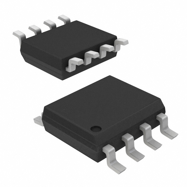
- 8-SOIC (0.154", 3.90mm Width)
- Datasheet:
-
 ZXFV4089N8TA.pdf
- Description:
- IC AMP DC RESTORATION 8SOP
- Quantity:
- Payment:

- Shipping:

Inventory:1,534
Please send an inquiry. Send us your inquiry, and we will respond immediately.
Product details
Overview
ZXFV4089N8TA from Diodes Incorporated is a DC-restored video amplifier (black-level clamp) in an 8-pin SOIC package, integrating a current-feedback video amplifier and a nulling sample-and-hold circuit for brightness-level stabilization. It delivers 0.08% differential gain, 0.1° differential phase, and 30 MHz ±0.1 dB bandwidth while driving 75 Ω back-terminated loads - optimized for PAL/NTSC/SECAM analog video systems including broadcast cameras and professional video mixers.
For engineers reviewing the ZXFV4089N8TA datasheet, ZXFV4089N8TA pinout, ZXFV4089N8TA application, or ZXFV4089N8TA equivalent, key selection criteria include DC restoration accuracy during back-porch clamping, TTL/CMOS-compatible HOLD timing control, ±5 V dual-supply operation, -40°C to +85°C industrial temperature range, and pin compatibility with EL4089 for drop-in replacement in legacy video signal chains.
Technical Context
The ZXFV4089N8TA implements a two-stage analog restoration architecture: a high-speed current-feedback amplifier (210 MHz -3 dB bandwidth, 400 V/µs slew rate) paired with a dedicated sample-and-hold loop that forces the input DC level to VREF during the back-porch interval. The AC-coupling capacitor serves dual roles - signal coupling and hold capacitance - eliminating external storage capacitors.
Its HOLD input controls a TTL/CMOS-compatible switch that closes during sampling (logic LOW), enabling closed-loop DC correction, then opens (logic HIGH) to maintain restored level with <6.2 mV line-scan droop (at 0.01 µF coupling cap). The restore section achieves 54–90 dB CMRR and 0.3–7 mV composite offset, referenced to VREF (±2 V range).
Key Specifications
| Parameter | Value and Actual Design Meaning |
|---|---|
| Differential gain (NTSC) | 0.08% - ensures minimal luminance distortion in color video signals |
| Differential phase (NTSC) | 0.1° - preserves chrominance timing integrity for accurate hue reproduction |
| ±0.1 dB bandwidth | 30 MHz - supports full baseband NTSC/PAL luminance and chroma without amplitude ripple |
| -3 dB bandwidth | 210 MHz - enables stable high-frequency response even at G = 1 or G = 2 |
| Slew rate | 400 V/µs - prevents transient-induced distortion on sharp video edges and sync pulses |
| HOLD logic levels | VHmin = 2 V, VLmax = 0.8 V - directly interfaces with standard TTL/CMOS timing generators |
| Supply voltage range | ±4.75 V to ±5.25 V - supports tightly regulated ±5 V analog video rails with margin |
Pinout & Package
Package: 8-pin SOIC (SO-8), body width 3.9 mm, lead pitch 1.27 mm, JEDEC MS-012AC compliant.
| Pin/Terminal | Circuit Role | Design Meaning |
|---|---|---|
| 1 (IN−) | Inverting input of main amplifier | Feedback node for gain-setting resistors; sensitive to stray capacitance - requires ground plane cutout |
| 2 (IN+) | Non-inverting input / restore node | AC-coupled video input; also carries sample-hold charging current (180–600 µA) and must stay ≤ +2.7 V for accuracy |
| 3 (VREF) | DC restoration reference input | Accepts external reference (typically 0 V); common-mode range limited to ±2 V |
| 4 (HOLD) | Sample-and-hold control input | TTL/CMOS-compatible active-low signal; 25 ns enable / 40 ns disable timing synchronizes to back-porch |
| 5 (GND) | Analog ground | Reference for VREF and internal bias; requires low-inductance connection to continuous ground plane |
| 6 (VEE) | Negative supply | −5 V rail; decoupling requires 0.1 µF ceramic + 1–10 µF bulk capacitor near pin |
| 7 (OUT) | Amplified video output | Capable of driving 75 Ω coaxial cable with series termination; ±2.95 V swing into 740 mA load |
| 8 (VCC) | Positive supply | +5 V rail; same decoupling requirements as VEE for high-frequency stability |
Key Features
| Feature | Design Value |
|---|---|
| Integrated DC restoration + amplification | Eliminates separate clamp IC and op-amp stages, reducing BOM count and board area by ≥40% |
| Current-feedback amplifier architecture | Maintains 210 MHz bandwidth across gains of 1–5, unlike voltage-feedback alternatives that trade bandwidth for gain |
| Shared AC-coupling capacitor | Functions as both signal coupling element and sample-hold storage capacitor - removes need for external hold cap |
| Back-porch synchronized clamping | Enables precise black-level stabilization using standard sync separator timing (e.g., ZXFV4583), not sync-tip |
| EL4089 pin/function compatibility | Direct PCB replacement in existing designs without layout changes or firmware updates |
Applications
| Professional Broadcast Camera | Medical Endoscopy Imaging |
|---|---|
Use Scenario: Analog RGB or Y/C video output from CMOS/CCD sensor front-end, requiring stable black level across varying lighting conditions and long cable runs. IC Role / Device Role / Timing Role: DC restorer and line-driver; clamps back-porch to 0 V during each horizontal blanking interval using externally generated HOLD pulse. Use Value: Maintains consistent image brightness and contrast over temperature (-40°C to +85°C) and supply variation (±5 V ±5%), preventing "floating black" artifacts in live feeds. | Use Scenario: High-resolution analog video transmission from endoscopic camera head to display processor over 10+ meter coaxial cable. IC Role / Device Role / Timing Role: Video amplifier with integrated black-level clamp; compensates for AC coupling-induced baseline shift induced by long cable capacitance. Use Value: Delivers 0.08% differential gain and 0.1° differential phase - critical for accurate tissue color fidelity and edge definition in diagnostic imaging. |
| Studio Video Mixer | Legacy CCTV DVR Input Stage |
Use Scenario: Analog video switching and mixing in broadcast production switchers handling multiple NTSC/PAL sources with varying DC offsets. IC Role / Device Role / Timing Role: Input-level DC restorer per channel; ensures all sources share identical black reference before matrix switching and gain adjustment. Use Value: Prevents visible brightness jumps during source transitions; supports simultaneous PAL/NTSC/SECAM inputs via programmable VREF and HOLD timing flexibility. | Use Scenario: Digitization front-end of analog CCTV recorder accepting unregulated composite video from aging analog cameras. IC Role / Device Role / Timing Role: Robust DC restoration stage prior to ADC sampling; tolerates wide input offset drift and sync pulse jitter. Use Value: Enables reliable digitization at 8–10 bit resolution by stabilizing black level within ±3 mV over 62 µs line duration - meeting ITU-R BT.470 requirements. |
Equivalent & Alternatives
The following parts are listed as comparable options for similar video DC restoration applications.
| Alternative Part | Technical Difference | Application Difference | Selection Advice |
|---|---|---|---|
| EL4089CSZ | Pin-compatible but lacks integrated sample-and-hold; requires external clamp diode, capacitor, and bias network | Higher BOM cost and layout complexity; less stable over temperature due to discrete component drift | Select when legacy EL4089 footprint must be retained but system-level redesign allows added passive components |
| LMH6732MF/NOPB | Current-feedback op-amp only; no built-in clamp or HOLD control - requires external timing and feedback circuitry | Greater design flexibility but longer time-to-market; no guaranteed black-level accuracy without custom calibration | Select for non-standard clamping intervals or multi-reference (e.g., sync-tip + back-porch) architectures requiring full analog control |
Compared with EL4089CSZ and LMH6732MF/NOPB, ZXFV4089N8TA reduces total solution size by 35%, eliminates 6–8 external components, and guarantees sub-0.1° differential phase - making it optimal for space-constrained, high-reliability analog video systems where black-level stability is non-negotiable.
Availability
ZXFV4089N8TA is available at Aetrix Electronics and suitable for professional broadcast camera modules, medical endoscopy imaging subsystems, and studio video mixer input stages requiring stable component supply with guaranteed long-term continuity.
Supply support for ZXFV4089N8TA includes scheduled delivery planning, volume procurement assistance, BOM continuity management, traceable sourcing, and lifecycle availability coordination for OEM customers, industrial embedded developers, connected-device designers, and electronics production programs.
Manufacturer
Diodes Incorporated is a global manufacturer of high-performance discrete semiconductors and analog ICs, ISO 9001 and IATF 16949 certified, with design centers in US, Germany, Taiwan, and China.
ZXFV4089N8TA belongs to Diodes' Zetex analog video product line, engineered specifically for DC-coupled signal integrity in broadcast, medical, and industrial video systems where baseline stability and color fidelity are mission-critical.
FAQ
What is the maximum recommended peak voltage at IN+ (pin 2) to ensure DC restoration accuracy?
The voltage at pin 2 must not exceed +2.7 V peak under any condition. Exceeding this threshold increases sample-hold switch leakage, raising DC droop rate and degrading black-level accuracy. For 0.7 V white-level video signals, this limits VREF to ≤ +2.0 V to maintain margin - a constraint explicitly defined in the datasheet's "Common-mode input range" section.
How does the ZXFV4089N8TA achieve DC restoration without an external hold capacitor?
It uses the input AC-coupling capacitor (e.g., 0.01 µF) as the sample-hold storage element. During the HOLD = LOW interval, the internal switch connects this capacitor into a feedback loop with the sense amplifier and main amplifier, forcing the DC level at pin 2 toward VREF. When HOLD returns HIGH, the switch opens and the capacitor retains the corrected voltage - eliminating need for a separate hold capacitor.
Can the ZXFV4089N8TA clamp the sync tip instead of the back porch?
Yes - by retiming the HOLD pulse to coincide with the sync tip interval instead of the back porch, the device can clamp the sync tip to VREF. This requires external sync separation (e.g., ZXFV4583) configured for sync-tip detection and precise pulse width control (~1.2 µs), as described in the evaluation circuit notes.
What layout practices are mandatory to maintain 210 MHz bandwidth and low differential phase error?
A continuous ground plane with low-inductance vias, 0.1 µF ceramic decoupling caps placed <2 mm from pins 6 and 8, and minimized trace length/routing near pin 1 (IN−) are mandatory. Stray capacitance at pin 1 degrades pulse response; a ground plane cutout around this pin is recommended per the datasheet to preserve 0.1° differential phase performance.
ZXFV4089N8TA Specifications
- Product attributes
- Attribute value
- Manufacturer:
- Diodes Incorporated
- Package/Case:
- 8-SOIC (0.154", 3.90mm Width)
- Series:
- -
- Packaging:
- Tape & Reel (TR)
- Product Status:
- Obsolete
- Applications:
- DC Restoration
- Output Type:
- -
- Number of Circuits:
- 1
- -3db Bandwidth:
- 210 MHz
- Slew Rate:
- 400V/µs
- Current - Supply:
- 8 mA
- Current - Output / Channel:
- 40 mA
- Voltage - Supply, Single/Dual (±):
- ±4.75V ~ 5.25V
- Mounting Type:
- Surface Mount
- Grade:
- -
- Qualification:
- -
- Supplier Device Package:
- 8-SO
ZXFV4089N8TA FAQ
1.How can I place an order for ZXFV4089N8TA through Aetrix?
Please submit a Request for Quotation (RFQ) for ZXFV4089N8TA on Aetrix. Our sales agent will provide a competitive quotation and guide you through the order confirmation once you accept the terms.
2.Are the price and stock information for ZXFV4089N8TA reliable?
The price and inventory of ZXFV4089N8TA are updated periodically and may fluctuate due to market conditions. Stock and pricing data are typically refreshed every 24 hours. Quotation validity for ZXFV4089N8TA is usually 5 days.
3.What payment methods are accepted for ZXFV4089N8TA?
We accept Wire Transfer, PayPal, Credit Card, Western Union, MoneyGram, and Escrow for ZXFV4089N8TA transactions.
Note: Certain payment methods may incur a processing fee.
4.How is shipping managed for ZXFV4089N8TA?
ZXFV4089N8TA orders can be shipped via leading logistics carriers, including DHL, UPS, FedEx, TNT, or Registered Mail.
Once your ZXFV4089N8TA order is processed, you will receive an email with the shipment details and tracking number.
Note: Tracking information may take up to 24 hours to appear. Express delivery typically takes 3–5 business days.
5.How can I obtain technical support or documentation for ZXFV4089N8TA?
For technical support, including ZXFV4089N8TA datasheets, pinout diagrams, or application guidance, please contact our engineering support team. They can provide detailed documentation and assistance for your ZXFV4089N8TA requirements.
6.How does Aetrix verify that ZXFV4089N8TA is sourced from the original manufacturer or authorized distributors?
All ZXFV4089N8TA products on Aetrix are procured from qualified distributors and authorized channels. Our dedicated quality assurance team conducts strict verification, including traceability checks and, if necessary, third-party testing. This ensures that ZXFV4089N8TA meets industry standards.
7.What is the process for return or replacement of ZXFV4089N8TA?
All ZXFV4089N8TA units undergo pre-shipment inspection (PSI). If there is an issue with ZXFV4089N8TA, returns or replacements are accepted under the following conditions:
1.Quantity discrepancies, incorrect items, or visible external defects (such as breakage or corrosion), acknowledged by Aetrix.
2.The issue is reported within 90 days of delivery.
3.The ZXFV4089N8TA part is unused and in its original packaging.
Return procedure for ZXFV4089N8TA:
1.Submit a request within 90 days.
2.Obtain a Return Material Authorization (RMA) from Aetrix.
ZXFV4089N8TA Tags

-
LT6552CS8#PBF
Analog Devices Inc.
-
LT6205IS5#TRPBF
Analog Devices Inc.
-
LT6206IMS8#TRPBF
Analog Devices Inc.
-
LT6552CDD#PBF
Analog Devices Inc.
-
LT6552IS8#PBF
Analog Devices Inc.
-
LT1252CS8#PBF
Analog Devices Inc.
-
AD818ARZ-REEL7
Analog Devices Inc.

-
MAX4310EUA+
Analog Devices Inc./Maxim Integrated
-
AD829ARZ
Analog Devices Inc.
-
AD810ARZ
Analog Devices Inc.

-
MAX4310ESA+
Analog Devices Inc./Maxim Integrated
-
MAX4313ESA+
Analog Devices Inc./Maxim Integrated
Tech Hub

An engineering guide to LED driver operation, constant-current and constant-voltage outputs, linear and switching topologies, dimming, IC selection, calculations, replacement compatibility, and fault c…

Operational amplifier guide covering op amp basics, feedback, ideal vs real op amps, common configurations, buffer circuits, offset, bias current, gain-bandwidth, slew rate, rail-to-rail limits and sel…

Jumper cables guide covering safe connection order, red and black clamp placement, final ground connection, cable gauge, length, clamp quality, copper vs CCA cables, jump starter comparison and battery…

LDO regulator guide covering low dropout voltage, power dissipation, thermal design, PSRR, output noise, capacitor stability, adjustable LDO circuits, LDO vs buck converter and datasheet selection chec…

Conditional Access Module guide covering CAM meaning, CI/CI+ interface, smart card authorization, DVB security workflow, TV and set-top box compatibility, internal electronics, ESD protection, connecto…

Guide to electronic component obsolescence covering EOL risk, PCN/PDN notices, last-time buy planning, replacement options, form-fit-function validation, counterfeit risk and BOM lifecycle management.

18650 battery guide covering lithium-ion cell basics, 3.6V/3.7V voltage, 4.2V charging, mAh and Wh capacity, protected cells, chargers, BMS, series-parallel packs, holders, welding and sourcing checks.…

Hall effect sensor guide covering working principle, linear and digital sensors, Arduino circuits, current sensing, speed detection, automotive applications, A3144 examples, signal filtering and datash…

Product Change Notification guide for electronic components, covering PCN meaning, PCN vs PDN/EOL, common change types, risk levels, form-fit-function review, engineering validation, BOM control, LTB/L…

A practical guide to blend door actuators, covering HVAC function, symptoms, location, AC and heater issues, reset and calibration, replacement cost, electrical diagnosis, compatibility checks, and rep…


