
 My Inquiry
 My Account


Diodes Incorporated ZXGD3114N7TC
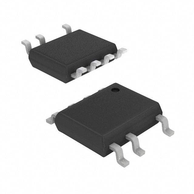
- Part No.:
- ZXGD3114N7TC
- Manufacturer:
- Diodes Incorporated
- Category:
- OR Controllers, Ideal Diodes
- Package:
- 8-SOIC (0.154", 3.90mm Width), 7 Leads
- Datasheet:
-
 ZXGD3114N7TC.pdf
- Description:
- OR'ING CONTROLLER SO-7 T&R 2.5K
- Quantity:
- Payment:

- Shipping:

Inventory:1,989
Please send an inquiry. Send us your inquiry, and we will respond immediately.
Product details
Overview
ZXGD3114N7TC from Diodes Incorporated is a 600V active ORing MOSFET controller in SO-7 package, designed to drive ultra-low RDS(ON) N-channel MOSFETs as ideal diodes in high- or low-side PSU configurations. It features a -3mV turn-off threshold (±2mV tolerance), <600ns turn-off time, and supports ±600V rail operation with <1mA quiescent current - enabling >98% power transfer efficiency in telecom redundant power systems.
For engineers reviewing the ZXGD3114N7TC datasheet, ZXGD3114N7TC pinout, ZXGD3114N7TC application, or ZXGD3114N7TC equivalent, key selection criteria include drain voltage rating (600V), gate drive sink/source capability (5A/2A), turn-off propagation delay (<400ns), and compatibility with high-voltage (±400V) ORing topologies in N+1 redundant servers.
Technical Context
The ZXGD3114N7TC implements a precision differential amplifier-based detector that monitors VDS across an external MOSFET to control gate drive state. Its turn-off threshold is fixed at -3mV with ±2mV tolerance, ensuring reliable reverse-current blocking even under temperature variation (-50°C to +150°C).
It integrates a high-current gate driver capable of 5A sink and 2A source peak current, with internal 12V gate clamp when VCC >12V. The device operates from 4V–20V VCC, supports both high-side (+400V) and low-side (-400V) configurations, and delivers <50mW standby power at 48V input.
Key Specifications
| Parameter | Value and Actual Design Meaning |
|---|---|
| Drain Voltage Rating | 600V - Enables direct connection to ±400V telecom/server bus rails without external level-shifting. |
| Turn-Off Threshold | -3mV (±2mV) - Detects sub-millivolt reverse conduction to block fault currents before bus collapse. |
| Turn-Off Propagation Delay | <400ns - Limits reverse current duration during PSU failure, preserving common bus stability. |
| Gate Sink/Source Current | 5A / 2A peak - Drives large-area MOSFET gates rapidly for <695ns rise and <131ns fall times (CL=47nF). |
| Quiescent Supply Current | 260µA typical - Enables <50mW standby consumption in 48V systems, critical for energy-efficient data centers. |
| VCC Range | 4V–20V - Supports direct bias from auxiliary rails or resistive dividers off HV buses. |
| Operating Temperature | -50°C to +150°C - Qualified for industrial and telecom environments with extended thermal margins. |
Pinout & Package
Package: SO-7 (Surface-mount, molded plastic, UL 94V-0, 0.074g weight, moisture sensitivity Level 1). Pin 1–7 arranged linearly with GND/GND/VCC/GATE/PGND/PGND/DRAIN configuration optimized for low-inductance high-current paths.
| Pin/Terminal | Circuit Role | Design Meaning |
|---|---|---|
| 1, 2 GND | Signal Ground Reference | Connects to MOSFET source and system ground; forms reference for differential VDS sensing. |
| 3 VCC | Power Supply Input | Accepts 4–20V supply; requires local X7R decoupling capacitor; primary thermal path for heat dissipation. |
| 4 GATE | MOSFET Gate Driver Output | Sources up to 2A / sinks up to 5A; clamped to 12V if VCC >12V; external RG sets turn-on speed. |
| 5, 6 PGND | Power Ground Return | Low-impedance return for high-current gate drive and MOSFET source; shares thermal pad with VCC. |
| 7 DRAIN | Drain Voltage Sense Input | Detects MOSFET VDS polarity and magnitude; triggers turn-off when VDS exceeds -3mV threshold. |
Key Features
| Feature | Design Value |
|---|---|
| Active ORing Control Logic | Differential amplifier with -3mV threshold enables precise, temperature-stable ideal diode behavior without external op-amps. |
| High-Voltage Rail Compatibility | 600V drain rating allows direct integration into ±400V telecom and server power buses without isolation components. |
| Ultra-Fast Fault Response | <600ns total turn-off time (tD(FALL) + tF) prevents reverse current from collapsing shared bus voltage during PSU faults. |
| Low-Power Standby Operation | 260µA IQ at 48V yields <50mW idle loss - critical for always-on infrastructure equipment meeting ENERGY STAR® Tier 2. |
| Thermally Optimized SO-7 Layout | Pins 3 (VCC) and 5–6 (PGND) serve as primary thermal conduction paths; recommended 10mm×10mm copper pads reduce RθJA to 191°C/W. |
Applications
| Telecom Redundant Power | Data Center Server Rails |
|---|---|
Use Scenario: Dual 48V PSUs feeding a common backplane bus in carrier-grade routers. IC Role / Device Role / Timing Role: High-side ORing controller detecting reverse current on failed PSU and disabling MOSFET within 600ns. Use Value: Prevents bus voltage droop below 44V during hot-swap events, maintaining uninterrupted packet forwarding. |
Use Scenario: N+1 redundant 12V intermediate bus architecture in AI accelerator racks. IC Role / Device Role / Timing Role: Low-side ORing controller managing parallel 12V outputs from multiple DC-DC modules. Use Value: Eliminates 0.4V forward drop per diode, reducing per-rail power loss by 3.2W at 8A load. |
| Industrial 400V DC Distribution | Network Equipment Hot-Swap |
Use Scenario: 400V DC microgrid powering distributed PLC controllers and I/O modules. IC Role / Device Role / Timing Role: High-side controller driving 600V MOSFETs to isolate faulty branch circuits. Use Value: Maintains >395V bus voltage during single-point failure, avoiding cascading shutdown of field devices. |
Use Scenario: Line-card hot-swap in modular switches with discharged output capacitors. IC Role / Device Role / Timing Role: Low-side ORing controller blocking inrush from charged bus into cold-inserted card. Use Value: Limits inrush current to <1.5A, preventing upstream fuse blow and bus sag during insertion. |
Equivalent & Alternatives
The following parts are listed as comparable options for similar active ORing controller applications.
| Alternative Part | Technical Difference | Application Difference | Selection Advice |
|---|---|---|---|
| LM5050-1MK/NOPB | 48V max VIN, 50mV turn-off threshold, no 600V drain rating | Limited to low-voltage DC distribution (≤48V); unsuitable for telecom HV rails | Select only for sub-50V systems where cost sensitivity outweighs HV capability. |
| TPS2412DR | 80V max VIN, adjustable threshold (10–100mV), 2.5µs turn-off | Requires external resistor network for threshold setting; too slow for 400V bus protection | Prefer for mid-voltage (24–80V) industrial controls where programmability justifies latency trade-off. |
Compared with LM5050-1MK/NOPB and TPS2412DR, the ZXGD3114N7TC uniquely supports ±400V rail operation with sub-millivolt threshold and nanosecond turn-off - making it the only viable choice for telecom and high-density server ORing where bus stability and efficiency are non-negotiable.
Availability
ZXGD3114N7TC is available at Aetrix Electronics and suitable for telecom power redundancy, data center server ORing, and industrial 400V DC distribution requiring stable component supply across multi-year production cycles.
Supply support for ZXGD3114N7TC includes scheduled delivery planning, volume procurement assistance, BOM continuity management, traceable sourcing, and lifecycle availability coordination for OEM customers, industrial embedded developers, connected-device designers, and electronics production programs.
Manufacturer
Diodes Incorporated is a global manufacturer of discrete semiconductors and analog ICs, headquartered in Plano, Texas, with design and manufacturing facilities across Asia and the Americas.
The ZXGD3114N7TC belongs to Diodes' high-voltage power management portfolio, engineered specifically for fault-tolerant ORing in telecom infrastructure and hyperscale data centers where reliability and efficiency at ±400V are mandatory.
FAQ
What is the maximum allowable VCC voltage for ZXGD3114N7TC?
The absolute maximum VCC is 25V, but the recommended operating range is 4V–20V. Exceeding 20V does not improve performance and risks exceeding thermal limits due to increased internal power dissipation. The gate driver clamps output to 12V above GND regardless of VCC, so higher supply voltages only increase quiescent loss without functional benefit.
Can ZXGD3114N7TC be used in high-side configuration with negative input rails?
Yes - the device supports true bipolar operation with drain voltage ranging from -3V to +600V relative to GND. In negative-rail applications (e.g., -48V telecom), the DRAIN pin connects to the negative bus, and the MOSFET is placed between bus and load, enabling ideal diode behavior for reverse-current blocking during source failure.
How does the -3mV turn-off threshold behave over temperature?
The threshold drift is ±2mV over full -50°C to +150°C range, confirmed by characterization data in DS40000 Rev.2. At 125°C, measured VT remains between -5mV and -1mV, ensuring consistent reverse-current detection without false triggering or delayed shutdown across industrial operating conditions.
Is external gate resistor required for stable operation?
An external gate resistor (RG) is optional but recommended to control MOSFET turn-on dV/dt and prevent oscillation. Typical values range from 1Ω to 10Ω depending on MOSFET Qg; values below 1Ω risk ringing, while >10Ω extends turn-on time beyond optimal efficiency. No resistor is needed for basic functionality, as the internal driver provides sufficient control.
ZXGD3114N7TC Specifications
- Product attributes
- Attribute value
- Manufacturer:
- Diodes Incorporated
- Series:
- -
- Package/Case:
- 8-SOIC (0.154", 3.90mm Width), 7 Leads
- Packaging:
- Tape & Reel (TR)
- Product Status:
- Active
- Type:
- -
- FET Type:
- -
- Ratio - Input:Output:
- -
- Internal Switch(s):
- -
- Delay Time - ON:
- -
- Delay Time - OFF:
- -
- Current - Output (Max):
- -
- Current - Supply:
- -
- Voltage - Supply:
- 4V ~ 20V
- Applications:
- -
- Operating Temperature:
- -50°C ~ 150°C (TJ)
- Grade:
- -
- Qualification:
- -
- Mounting Type:
- Surface Mount
- Supplier Device Package:
- 7-SO
ZXGD3114N7TC FAQ
1.How can I place an order for ZXGD3114N7TC through Aetrix?
Please submit a Request for Quotation (RFQ) for ZXGD3114N7TC on Aetrix. Our sales agent will provide a competitive quotation and guide you through the order confirmation once you accept the terms.
2.Are the price and stock information for ZXGD3114N7TC reliable?
The price and inventory of ZXGD3114N7TC are updated periodically and may fluctuate due to market conditions. Stock and pricing data are typically refreshed every 24 hours. Quotation validity for ZXGD3114N7TC is usually 5 days.
3.What payment methods are accepted for ZXGD3114N7TC?
We accept Wire Transfer, PayPal, Credit Card, Western Union, MoneyGram, and Escrow for ZXGD3114N7TC transactions.
Note: Certain payment methods may incur a processing fee.
4.How is shipping managed for ZXGD3114N7TC?
ZXGD3114N7TC orders can be shipped via leading logistics carriers, including DHL, UPS, FedEx, TNT, or Registered Mail.
Once your ZXGD3114N7TC order is processed, you will receive an email with the shipment details and tracking number.
Note: Tracking information may take up to 24 hours to appear. Express delivery typically takes 3–5 business days.
5.How can I obtain technical support or documentation for ZXGD3114N7TC?
For technical support, including ZXGD3114N7TC datasheets, pinout diagrams, or application guidance, please contact our engineering support team. They can provide detailed documentation and assistance for your ZXGD3114N7TC requirements.
6.How does Aetrix verify that ZXGD3114N7TC is sourced from the original manufacturer or authorized distributors?
All ZXGD3114N7TC products on Aetrix are procured from qualified distributors and authorized channels. Our dedicated quality assurance team conducts strict verification, including traceability checks and, if necessary, third-party testing. This ensures that ZXGD3114N7TC meets industry standards.
7.What is the process for return or replacement of ZXGD3114N7TC?
All ZXGD3114N7TC units undergo pre-shipment inspection (PSI). If there is an issue with ZXGD3114N7TC, returns or replacements are accepted under the following conditions:
1.Quantity discrepancies, incorrect items, or visible external defects (such as breakage or corrosion), acknowledged by Aetrix.
2.The issue is reported within 90 days of delivery.
3.The ZXGD3114N7TC part is unused and in its original packaging.
Return procedure for ZXGD3114N7TC:
1.Submit a request within 90 days.
2.Obtain a Return Material Authorization (RMA) from Aetrix.
ZXGD3114N7TC Tags

-
LM66100DCKR
Texas Instruments
-
LM66200DRLR
Texas Instruments
-
LM66100DCKT
Texas Instruments

-
AP74700QW6-7
Diodes Incorporated
-
LM73100RPWR
Texas Instruments
-
LM74502DDFR
Texas Instruments
-
LM74700QDBVRQ1
Texas Instruments
-
MAX40200AUK+T
Analog Devices Inc./Maxim Integrated
-
MAX40200ANS+T
Analog Devices Inc./Maxim Integrated
-
MAX40203AUK+T
Analog Devices Inc./Maxim Integrated
-
MAX40203ANS+T
Analog Devices Inc./Maxim Integrated
-
LM74502QDDFRQ1
Texas Instruments
Tech Hub

Jumper cables guide covering safe connection order, red and black clamp placement, final ground connection, cable gauge, length, clamp quality, copper vs CCA cables, jump starter comparison and battery…

LDO regulator guide covering low dropout voltage, power dissipation, thermal design, PSRR, output noise, capacitor stability, adjustable LDO circuits, LDO vs buck converter and datasheet selection chec…

Conditional Access Module guide covering CAM meaning, CI/CI+ interface, smart card authorization, DVB security workflow, TV and set-top box compatibility, internal electronics, ESD protection, connecto…

Guide to electronic component obsolescence covering EOL risk, PCN/PDN notices, last-time buy planning, replacement options, form-fit-function validation, counterfeit risk and BOM lifecycle management.

18650 battery guide covering lithium-ion cell basics, 3.6V/3.7V voltage, 4.2V charging, mAh and Wh capacity, protected cells, chargers, BMS, series-parallel packs, holders, welding and sourcing checks.…

Hall effect sensor guide covering working principle, linear and digital sensors, Arduino circuits, current sensing, speed detection, automotive applications, A3144 examples, signal filtering and datash…

Product Change Notification guide for electronic components, covering PCN meaning, PCN vs PDN/EOL, common change types, risk levels, form-fit-function review, engineering validation, BOM control, LTB/L…

A practical guide to blend door actuators, covering HVAC function, symptoms, location, AC and heater issues, reset and calibration, replacement cost, electrical diagnosis, compatibility checks, and rep…

Engineering guide to Raspberry Pi alternatives, covering chip-level differences, Orange Pi, ROCK, Jetson, Banana Pi, NanoPi, Compute Module, Pico, GPIO, camera, HAT compatibility, and replacement risks…

Engineering guide to dynamic load response testing for high-current buck converters, covering load step setup, slew rate, Vcore undershoot, overshoot, recovery time, probe location, output capacitors a…


