
 My Inquiry
 My Account


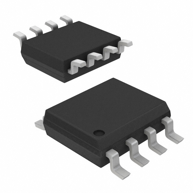
Diodes Incorporated ZXSC100N8TC
- Part No.:
- ZXSC100N8TC
- Manufacturer:
- Diodes Incorporated
- Category:
- DC DC Switching Controllers
- Package:
- 8-SOIC (0.154", 3.90mm Width)
- Datasheet:
-
 ZXSC100N8TC.pdf
- Description:
- IC REG CTRLR BOOST 8SOIC
- Quantity:
- Payment:

- Shipping:

Inventory:3,160
Please send an inquiry. Send us your inquiry, and we will respond immediately.
Product details
Overview
ZXSC100N8TC from Diodes Incorporated is a non-synchronous PFM DC-DC controller IC designed for single-cell NiCd/NiMH battery systems, enabling step-up conversion from as low as 0.926 V input. It delivers adjustable output voltage (≥VIN) via external resistive feedback, achieves 82% efficiency at 1 V input, and draws only 150 µA quiescent current-optimized for portable medical devices, GPS receivers, and digital cameras.
For engineers reviewing the ZXSC100N8TC datasheet, ZXSC100N8TC pinout, ZXSC100N8TC application, or ZXSC100N8TC equivalent, key selection criteria include minimum startup voltage (1.01 V), FB reference (730 mV), ISENSE threshold (25 mV), VDRIVE drive capability (5–10 mA), and SO-8 thermal performance (780 mW @ 25°C).
Technical Context
The ZXSC100N8TC implements pulse-frequency modulation with a fixed off-time monostable (1.7–3 µs) and dual-comparator regulation: Comp1 controls switching based on FB voltage vs. 730 mV reference, while Comp2 terminates conduction when ISENSE exceeds 25 mV. Its shutdown circuit activates at VCC = 1.01 V with 80 mV hysteresis.
It operates in discontinuous conduction mode with constant pulse width and variable frequency, relying on an external NPN switching transistor and Schottky diode. Drive current is set by an external resistor between RE and VCC, referenced to VCC − 25 mV, and VDRIVE supplies base current up to 10 mA to the external transistor.
Key Specifications
| Parameter | Value and Actual Design Meaning |
|---|---|
| Startup Voltage | 1.01 V - enables reliable operation from depleted NiMH cells without brown-out reset |
| Min Operating Input | 0.926 V - supports full-load regulation down to near-dead battery state |
| FB Reference Voltage | 730 mV ±22 mV - sets output via RA/RB divider; defines precision of adjustable VOUT |
| ISENSE Threshold | 25 mV - determines peak inductor current limit and overcurrent protection point |
| Quiescent Current | 150 µA - minimizes no-load battery drain in standby mode |
| VDRIVE Output | VCC − 0.17 V @ 5 mA - ensures sufficient base drive margin for external NPN saturation |
| Max Power Dissipation | 780 mW in SO-8 - constrains continuous output power under 70°C ambient |
Pinout & Package
Package: SO-8, RoHS-compliant "Green" molding compound with lead-free finish.
| Pin/Terminal | Circuit Role | Design Meaning |
|---|---|---|
| 1 EM | Emitter monitor | Connects to RE in low-power configs; left open in high-current designs to bypass internal emitter path |
| 2 BAS | Base assist enable | Drives external PNP to boost VDRIVE current when main NPN requires >10 mA base drive |
| 3 RE | Drive current sense | Sets VDRIVE current via external resistor; threshold = VCC − 25 mV |
| 4 VCC | Input supply | Accepts 0.926–3.5 V; powers internal circuitry and serves as reference for RE/VDREF |
| 5 ISENSE | Current limit sense | Detects external sense resistor voltage; triggers turn-off at 25 mV |
| 6 FB | Output voltage feedback | Compares divided VOUT to 730 mV reference to regulate output |
| 7 GND | Ground reference | Common return for all internal circuits and external sense components |
| 8 VDRIVE | External transistor driver | Supplies controlled base current to external NPN; max 10 mA sink capability |
Key Features
| Feature | Design Value |
|---|---|
| Ultra-low startup voltage | 1.01 V ensures functional operation even with deeply discharged NiMH cells (≤1.0 V) |
| Adjustable output range | VOUT ≥ VIN - supports flexible rail generation without fixed-output constraint |
| Programmable current limit | 25 mV ISENSE threshold + external RSENSE enables precise IPK tuning for thermal safety |
| Low-noise PFM control | Variable-frequency operation avoids fixed switching noise peaks; ideal for RF-sensitive applications like GPS |
| Thermal-aware packaging | SO-8 with 780 mW PD rating allows 100+ mA output in compact footprint without forced cooling |
Applications
| Portable Medical Devices | Digital Cameras |
|---|---|
Use Scenario: Powering LED flash drivers and image sensor bias rails from a single NiMH cell in compact handheld diagnostics units. IC Role / Device Role / Timing Role: DC-DC controller regulating 3.3 V or 5 V output with tight load transient response during burst-mode imaging. Use Value: 82% efficiency at 1 V input extends battery life by >30% versus linear regulators in intermittent-use scenarios. | Use Scenario: Supplying CCD/CMOS sensor logic and autofocus motor drivers in sub-100g consumer cameras. IC Role / Device Role / Timing Role: Adjustable boost controller delivering stable 3.3 V from 1.2 V nominal NiMH input, rejecting battery voltage sag during flash charging. Use Value: 150 µA quiescent current prevents >5% monthly self-discharge-critical for shelf-ready devices. |
| GPS Receivers | Electronic Toothbrushes |
Use Scenario: Generating clean 3.0 V supply for RF front-end and baseband processor in battery-powered handheld navigation units. IC Role / Device Role / Timing Role: Low-noise PFM controller minimizing conducted EMI into sensitive L1-band RF paths. Use Value: Variable-frequency operation avoids spectral concentration at fixed harmonics-reducing GPS position error by <2 m CEP. | Use Scenario: Driving vibration motor and LED status indicators from a sealed 1.2 V NiMH cell in waterproof oral care devices. IC Role / Device Role / Timing Role: High-efficiency boost controller sustaining 5 V motor pulses despite rapid battery voltage decay during 2-minute cycles. Use Value: 0.926 V minimum operating voltage enables full runtime from fresh to fully depleted cell (1.4 V → 0.95 V). |
Equivalent & Alternatives
The following parts are listed as comparable options for similar DC-DC controller applications.
| Alternative Part | Technical Difference | Application Difference | Selection Advice |
|---|---|---|---|
| MAX756CPA+ | Fixed 3.3 V/5 V outputs; higher 100 µA quiescent current; requires external MOSFET | Lacks adjustable VOUT; less suitable for multi-rail systems needing custom voltages | Prefer when fixed output simplifies BOM and layout; avoid if VOUT flexibility is required |
| TPS61099YFFR | Integrated MOSFET; 300 nA IQ; 0.7 V startup; synchronous rectification | Higher integration reduces external component count but increases cost and limits max output voltage to 5.5 V | Choose for ultra-low-power IoT sensors; not recommended for >2 W loads or >20 V outputs |
Compared with MAX756CPA+ and TPS61099YFFR, the ZXSC100N8TC uniquely balances ultra-low startup voltage (1.01 V), user-adjustable output (≥VIN), and SO-8 thermal capability-making it optimal for cost-sensitive, medium-power (≤2 W), single-cell NiMH/NiCd systems requiring design flexibility.
Availability
ZXSC100N8TC is available at Aetrix Electronics and suitable for portable medical devices, GPS receivers, digital cameras, and electronic toothbrushes requiring stable component supply across long-lifecycle consumer and industrial programs.
Supply support for ZXSC100N8TC includes scheduled delivery planning, volume procurement assistance, BOM continuity management, traceable sourcing, and lifecycle availability coordination for OEM customers, industrial embedded developers, connected-device designers, and electronics production programs.
Manufacturer
Diodes Incorporated is a global manufacturer of discrete semiconductors and analog ICs, specializing in high-reliability power management, signal integrity, and protection solutions for consumer, industrial, and automotive markets.
The ZXSC100 series belongs to Diodes' low-voltage DC-DC controller product line, engineered specifically for energy-constrained single-cell battery applications where startup robustness and quiescent current efficiency are critical system-level requirements.
FAQ
What is the minimum input voltage required for ZXSC100N8TC to start regulation?
The ZXSC100N8TC starts regulation at VCC = 1.01 V (typical) with 80 mV hysteresis, and maintains full-load regulation down to 0.926 V. This enables operation from nearly exhausted NiMH cells, unlike most boost controllers requiring ≥1.8 V startup. The internal shutdown comparator triggers reliably across temperature and process variation per DS33613 Rev. 6-2.
How is output voltage adjusted on the ZXSC100N8TC?
Output voltage is set using an external resistive divider from VOUT to GND, connected to the FB pin. With VFB = 730 mV (±22 mV), VOUT = 730 mV × (1 + RA/RB). Resistor values must ensure FB input current ≤200 nA to minimize battery drain; typical designs use RB = 100 kΩ and scale RA accordingly.
Can ZXSC100N8TC drive a MOSFET instead of a bipolar transistor?
No-the ZXSC100N8TC's VDRIVE output is optimized for bipolar NPN base drive (5–10 mA sink), not MOSFET gate charging. Its drive strength and voltage swing (VCC − 0.17 V) lack the dV/dt and peak current needed for efficient MOSFET switching. The datasheet explicitly specifies NPN transistor Q1 and provides base-drive equations for bipolar devices only.
What is the role of the ISENSE pin and how is its threshold used?
The ISENSE pin monitors voltage across an external sense resistor in series with the switching transistor's emitter. At 25 mV (typical), it triggers immediate turn-off of VDRIVE to limit peak inductor current. This sets the converter's current limit and protects against short-circuit or overload conditions-critical for battery safety and thermal management in portable systems.
ZXSC100N8TC Specifications
- Product attributes
- Attribute value
- Manufacturer:
- Diodes Incorporated
- Series:
- -
- Package/Case:
- 8-SOIC (0.154", 3.90mm Width)
- Packaging:
- Tape & Reel (TR)
- Product Status:
- Obsolete
- Output Type:
- Transistor Driver
- Function:
- Step-Up
- Output Configuration:
- Positive
- Topology:
- Boost
- Number of Outputs:
- 1
- Output Phases:
- 1
- Voltage - Supply (Vcc/Vdd):
- 0.98V ~ 3.5V
- Frequency - Switching:
- 200kHz
- Duty Cycle (Max):
- -
- Synchronous Rectifier:
- No
- Clock Sync:
- No
- Serial Interfaces:
- -
- Control Features:
- -
- Operating Temperature:
- 0°C ~ 70°C (TA)
- Grade:
- -
- Qualification:
- -
- Mounting Type:
- Surface Mount
- Supplier Device Package:
- 8-SO
ZXSC100N8TC FAQ
1.How can I place an order for ZXSC100N8TC through Aetrix?
Please submit a Request for Quotation (RFQ) for ZXSC100N8TC on Aetrix. Our sales agent will provide a competitive quotation and guide you through the order confirmation once you accept the terms.
2.Are the price and stock information for ZXSC100N8TC reliable?
The price and inventory of ZXSC100N8TC are updated periodically and may fluctuate due to market conditions. Stock and pricing data are typically refreshed every 24 hours. Quotation validity for ZXSC100N8TC is usually 5 days.
3.What payment methods are accepted for ZXSC100N8TC?
We accept Wire Transfer, PayPal, Credit Card, Western Union, MoneyGram, and Escrow for ZXSC100N8TC transactions.
Note: Certain payment methods may incur a processing fee.
4.How is shipping managed for ZXSC100N8TC?
ZXSC100N8TC orders can be shipped via leading logistics carriers, including DHL, UPS, FedEx, TNT, or Registered Mail.
Once your ZXSC100N8TC order is processed, you will receive an email with the shipment details and tracking number.
Note: Tracking information may take up to 24 hours to appear. Express delivery typically takes 3–5 business days.
5.How can I obtain technical support or documentation for ZXSC100N8TC?
For technical support, including ZXSC100N8TC datasheets, pinout diagrams, or application guidance, please contact our engineering support team. They can provide detailed documentation and assistance for your ZXSC100N8TC requirements.
6.How does Aetrix verify that ZXSC100N8TC is sourced from the original manufacturer or authorized distributors?
All ZXSC100N8TC products on Aetrix are procured from qualified distributors and authorized channels. Our dedicated quality assurance team conducts strict verification, including traceability checks and, if necessary, third-party testing. This ensures that ZXSC100N8TC meets industry standards.
7.What is the process for return or replacement of ZXSC100N8TC?
All ZXSC100N8TC units undergo pre-shipment inspection (PSI). If there is an issue with ZXSC100N8TC, returns or replacements are accepted under the following conditions:
1.Quantity discrepancies, incorrect items, or visible external defects (such as breakage or corrosion), acknowledged by Aetrix.
2.The issue is reported within 90 days of delivery.
3.The ZXSC100N8TC part is unused and in its original packaging.
Return procedure for ZXSC100N8TC:
1.Submit a request within 90 days.
2.Obtain a Return Material Authorization (RMA) from Aetrix.
ZXSC100N8TC Tags

-
UCC28C45DR
Texas Instruments
-
UCC28C40DR
Texas Instruments
-
UCC28C43DR
Texas Instruments

-
ZXSC410E6TA
Diodes Incorporated

-
LM3524DMX/NOPB
Texas Instruments

-
LM3489MMX/NOPB
Texas Instruments
-
MIC2102YML-TR
Microchip Technology

-
LM5148RGYR
Texas Instruments
-
TL598CDR
Texas Instruments

-
LM5155DSSR
Texas Instruments

-
LM25085MYX/NOPB
Texas Instruments
-
UCC2813DTR-0
Texas Instruments
Tech Hub

Operational amplifier guide covering op amp basics, feedback, ideal vs real op amps, common configurations, buffer circuits, offset, bias current, gain-bandwidth, slew rate, rail-to-rail limits and sel…

Jumper cables guide covering safe connection order, red and black clamp placement, final ground connection, cable gauge, length, clamp quality, copper vs CCA cables, jump starter comparison and battery…

LDO regulator guide covering low dropout voltage, power dissipation, thermal design, PSRR, output noise, capacitor stability, adjustable LDO circuits, LDO vs buck converter and datasheet selection chec…

Conditional Access Module guide covering CAM meaning, CI/CI+ interface, smart card authorization, DVB security workflow, TV and set-top box compatibility, internal electronics, ESD protection, connecto…

Guide to electronic component obsolescence covering EOL risk, PCN/PDN notices, last-time buy planning, replacement options, form-fit-function validation, counterfeit risk and BOM lifecycle management.

18650 battery guide covering lithium-ion cell basics, 3.6V/3.7V voltage, 4.2V charging, mAh and Wh capacity, protected cells, chargers, BMS, series-parallel packs, holders, welding and sourcing checks.…

Hall effect sensor guide covering working principle, linear and digital sensors, Arduino circuits, current sensing, speed detection, automotive applications, A3144 examples, signal filtering and datash…

Product Change Notification guide for electronic components, covering PCN meaning, PCN vs PDN/EOL, common change types, risk levels, form-fit-function review, engineering validation, BOM control, LTB/L…

A practical guide to blend door actuators, covering HVAC function, symptoms, location, AC and heater issues, reset and calibration, replacement cost, electrical diagnosis, compatibility checks, and rep…

Engineering guide to Raspberry Pi alternatives, covering chip-level differences, Orange Pi, ROCK, Jetson, Banana Pi, NanoPi, Compute Module, Pico, GPIO, camera, HAT compatibility, and replacement risks…


