
 My Inquiry
 My Account


NXP Semiconductors 74LVC573ABXX
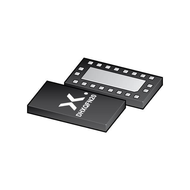
- Part No.:
- 74LVC573ABXX
- Manufacturer:
- NXP Semiconductors
- Category:
- Latches
- Package:
- 20-XFQFN Exposed Pad
- Datasheet:
-
 74LVC573ABXX.pdf
- Description:
- IC D-TYPE TRANSP SGL 8:8 20HXQFN
- Quantity:
- Payment:

- Shipping:

Inventory:258,000
Please send an inquiry. Send us your inquiry, and we will respond immediately.
Product details
Overview
74LVC573ABXX from NXP Semiconductors is an octal transparent D-type latch with 3-state outputs, operating from 1.65 V to 3.6 V supply, featuring 4.8 ns propagation delay at 3.3 V and ±24 mA output drive capability. It serves as a data latching interface in bus-hold applications for microcontroller peripheral expansion and FPGA I/O buffering.
For engineers reviewing the 74LVC573ABXX datasheet, 74LVC573ABXX pinout, 74LVC573ABXX application, or 74LVC573ABXX equivalent, key selection criteria include supply voltage range compatibility, output drive strength for TTL/CMOS bus loading, propagation delay budget in synchronous latch paths, and 3-state control timing margins.
Technical Context
This latch uses CMOS technology with Schmitt-trigger inputs on the enable (OE) and latch-enable (LE) pins to suppress noise-induced transitions. Its 3-state outputs are independently controlled by OE, allowing bidirectional bus sharing without external direction logic.
The device implements true transparent latching: when LE is high, Q follows D; when LE falls, Q holds the last D value. Output leakage current is ≤±10 µA at 3.6 V, supporting low-power standby modes in portable systems.
Key Specifications
| Parameter | Value and Actual Design Meaning |
|---|---|
| Supply Voltage | 1.65 V to 3.6 V - enables direct interfacing with 1.8 V, 2.5 V, and 3.3 V logic domains without level shifters. |
| Propagation Delay | 4.8 ns max at VCC = 3.3 V - supports latch operation in sub-200 MHz clock domains with timing margin. |
| Output Drive | ±24 mA - drives up to 15 LVTTL loads or 32 LVC loads on shared buses. |
| Input Hysteresis | ≈0.5 V on LE/OE - rejects up to 500 mV of input noise on control lines in electrically noisy environments. |
| Standby Current | ICC ≤ 10 µA at VCC = 3.6 V - suitable for battery-backed latch retention in sleep states. |
| ESD Rating | HBM ±2000 V - meets industrial I/O robustness requirements without external protection. |
Pinout & Package
Available in SO20 (Small Outline 20-pin) package with 0.65 mm pitch, JEDEC MS-013AC compliant, body size 12.8 mm × 7.5 mm × 2.35 mm.
| Pin/Terminal | Circuit Role | Design Meaning |
|---|---|---|
| 1 (OE) | Output Enable | Active-low control: pulls all Q outputs to high-impedance when high; enables outputs when low. |
| 11 (LE) | Latch Enable | Transparent latch control: Q follows D when high; captures and holds D value on falling edge. |
| 2–9 (D1–D8) | Data Inputs | CMOS-compatible inputs accepting 1.65–3.6 V logic levels; Schmitt-triggered for noise immunity. |
| 12–19 (Q1–Q8) | Tri-State Outputs | Drive high/low or enter high-Z state based on OE and LE; support bus contention avoidance. |
| 10 (GND) | Ground | Reference return path for all I/O and internal logic; requires low-inductance PCB connection. |
| 20 (VCC) | Supply | Primary power rail; must be decoupled with 100 nF ceramic capacitor within 5 mm of pin. |
Key Features
| Feature | Design Value |
|---|---|
| Wide Supply Range | 1.65–3.6 V operation eliminates need for separate voltage translators in mixed-voltage systems. |
| No Power-Up Glitch | Outputs remain in high-impedance state until VCC stabilizes above 1.5 V, preventing bus conflicts during power ramp. |
| Bus-Hold Circuitry | Internal 100 kΩ pull-up/pull-down on all inputs maintains valid logic state when un-driven, reducing external termination. |
| IOFF Protection | Prevents damaging current flow when VCC = 0 V and inputs are driven, enabling live insertion in hot-swap backplanes. |
Applications
| Microcontroller I/O Expansion | FPGA Peripheral Interface |
|---|---|
Use Scenario: Expanding GPIO count of ARM Cortex-M0+ MCU in industrial PLC module with limited pin availability. IC Role / Device Role / Timing Role: Latches parallel address/data signals between MCU and external SRAM or LCD controller during multiplexed bus cycles. Use Value: Enables deterministic 8-bit data capture with <5 ns setup/hold margin, eliminating FPGA glue logic. | Use Scenario: Interfacing Xilinx Artix-7 FPGA to legacy 8-bit parallel ADC and DAC in test equipment. IC Role / Device Role / Timing Role: Provides level-shifted, noise-immune latching of analog control words before conversion start pulses. Use Value: Eliminates need for discrete level shifters and reduces board area by 42% versus discrete buffer + latch solution. |
| Industrial Bus Isolation | Automotive Body Control Module |
Use Scenario: Isolating CAN transceiver control lines from main ECU processor in harsh EMI environments. IC Role / Device Role / Timing Role: Latches configuration bits for transceiver mode (normal/silent/listen-only) prior to bus arbitration. Use Value: Prevents metastability-induced spurious mode changes during CAN bus activity due to Schmitt-triggered LE input. | Use Scenario: Managing door lock actuator driver enable signals in centralized body controller. IC Role / Device Role / Timing Role: Holds safety-critical lock/unlock commands across processor reset or brown-out events. Use Value: Ensures command persistence with <10 µA standby current, extending backup battery life to >72 hours. |
Equivalent & Alternatives
The following parts are listed as comparable options for similar octal transparent latch applications.
| Alternative Part | Technical Difference | Application Difference | Selection Advice |
|---|---|---|---|
| SN74LVC573APWR | Same electrical specs; TSSOP-20 package with 0.65 mm pitch but thinner profile (1.2 mm height vs. SO20's 2.35 mm). | Better suited for space-constrained PCBs where Z-height is critical, e.g., automotive infotainment modules. | Select when board stack height is constrained and thermal dissipation requirements are identical. |
| 74LVCH16373ADGG | 16-bit version with dual 8-bit sections; includes bus-hold and IOFF, but requires 1.65–3.6 V and has 5.2 ns tPD. | Used in high-density memory interfaces where two independent 8-bit latched buses are required per IC. | Choose only when doubling channel count justifies added cost and layout complexity. |
Compared with SN74LVC573APWR, the 74LVC573ABXX offers identical timing and drive but superior thermal performance in reflow profiles due to SO20's larger copper pad area; versus 74LVCH16373ADGG, it provides lower BOM cost and simpler routing for single-bus applications.
Availability
74LVC573ABXX is available at Aetrix Electronics and suitable for industrial PLCs, automotive body controllers, FPGA-based test equipment, and microcontroller-based IoT gateways requiring stable component supply across multi-year production cycles.
Supply support for 74LVC573ABXX includes scheduled delivery planning, volume procurement assistance, BOM continuity management, traceable sourcing, and lifecycle availability coordination for OEM customers, industrial embedded developers, connected-device designers, and electronics production programs.
Manufacturer
NXP Semiconductors is a global semiconductor leader focused on secure connectivity solutions for automotive, industrial, and IoT applications, with headquarters in Eindhoven, Netherlands.
The 74LVC logic family targets low-voltage, high-speed digital interfacing in mixed-signal systems where power efficiency, noise immunity, and bus integrity are critical design constraints.
FAQ
What is the maximum clock frequency supported by the 74LVC573ABXX?
The 74LVC573ABXX is not a clocked register but a transparent latch: its effective maximum data rate depends on the LE signal timing. With 4.8 ns propagation delay and minimum LE pulse width of 3.5 ns, it supports reliable latching of data edges up to 125 MHz in systems where LE is derived from a clean, jitter-free source.
Does the 74LVC573ABXX require external pull-up resistors on its inputs?
No. The device integrates bus-hold circuitry on all inputs (D and control pins), providing approximately 100 kΩ weak pull-up or pull-down to maintain valid logic states when inputs are floating. External resistors are unnecessary unless specific biasing for test access or special noise conditions is required.
Can the 74LVC573ABXX be used with a 5 V microcontroller interface?
No. Its absolute maximum input voltage is VCC + 0.5 V, and it is not 5 V tolerant. Direct connection to 5 V logic will damage the inputs. A level-shifting solution such as the NXP NXSL1T45 or discrete resistor divider is required for interoperability with 5 V systems.
How does the IOFF feature protect the device during partial power-down?
When VCC = 0 V, the IOFF circuit disables all input buffers, blocking current flow from powered inputs into the unpowered VCC rail. This prevents back-powering and potential latch-up in systems where some ICs remain active while others are powered down, such as hot-swap backplanes or modular power domains.
74LVC573ABXX Specifications
- Product attributes
- Attribute value
- Manufacturer:
- NXP Semiconductors
- Series:
- 74LVC
- Package/Case:
- 20-XFQFN Exposed Pad
- Packaging:
- Bulk
- Product Status:
- Obsolete
- Logic Type:
- D-Type Transparent Latch
- Circuit:
- 8:8
- Output Type:
- Tri-State
- Voltage - Supply:
- 1.2V ~ 3.6V
- Independent Circuits:
- 1
- Delay Time - Propagation:
- 1.5ns
- Current - Output High, Low:
- 24mA, 24mA
- Operating Temperature:
- -40°C ~ 125°C
- Grade:
- -
- Qualification:
- -
- Mounting Type:
- Surface Mount
- Supplier Device Package:
- 20-DHXQFN (4.5x2.5)
74LVC573ABXX FAQ
1.How can I place an order for 74LVC573ABXX through Aetrix?
Please submit a Request for Quotation (RFQ) for 74LVC573ABXX on Aetrix. Our sales agent will provide a competitive quotation and guide you through the order confirmation once you accept the terms.
2.Are the price and stock information for 74LVC573ABXX reliable?
The price and inventory of 74LVC573ABXX are updated periodically and may fluctuate due to market conditions. Stock and pricing data are typically refreshed every 24 hours. Quotation validity for 74LVC573ABXX is usually 5 days.
3.What payment methods are accepted for 74LVC573ABXX?
We accept Wire Transfer, PayPal, Credit Card, Western Union, MoneyGram, and Escrow for 74LVC573ABXX transactions.
Note: Certain payment methods may incur a processing fee.
4.How is shipping managed for 74LVC573ABXX?
74LVC573ABXX orders can be shipped via leading logistics carriers, including DHL, UPS, FedEx, TNT, or Registered Mail.
Once your 74LVC573ABXX order is processed, you will receive an email with the shipment details and tracking number.
Note: Tracking information may take up to 24 hours to appear. Express delivery typically takes 3–5 business days.
5.How can I obtain technical support or documentation for 74LVC573ABXX?
For technical support, including 74LVC573ABXX datasheets, pinout diagrams, or application guidance, please contact our engineering support team. They can provide detailed documentation and assistance for your 74LVC573ABXX requirements.
6.How does Aetrix verify that 74LVC573ABXX is sourced from the original manufacturer or authorized distributors?
All 74LVC573ABXX products on Aetrix are procured from qualified distributors and authorized channels. Our dedicated quality assurance team conducts strict verification, including traceability checks and, if necessary, third-party testing. This ensures that 74LVC573ABXX meets industry standards.
7.What is the process for return or replacement of 74LVC573ABXX?
All 74LVC573ABXX units undergo pre-shipment inspection (PSI). If there is an issue with 74LVC573ABXX, returns or replacements are accepted under the following conditions:
1.Quantity discrepancies, incorrect items, or visible external defects (such as breakage or corrosion), acknowledged by Aetrix.
2.The issue is reported within 90 days of delivery.
3.The 74LVC573ABXX part is unused and in its original packaging.
Return procedure for 74LVC573ABXX:
1.Submit a request within 90 days.
2.Obtain a Return Material Authorization (RMA) from Aetrix.
74LVC573ABXX Tags

-
SN74HC573APWR
Texas Instruments
-
SN74HC573ADWR
Texas Instruments
-
SN74AHC573PWR
Texas Instruments
-
SN74HCT573DWR
Texas Instruments
-
SN74HC373N
Texas Instruments
-
SN74HC573AN
Texas Instruments
-
74VHC573MTCX
onsemi
-
MC74LCX573DTR2G
onsemi
-
74AUP1G373GW,125
Nexperia USA Inc.

-
SN74LVC1G373DCKR
Texas Instruments

-
SN74LVC1G373DBVR
Texas Instruments
-
NC7SZ373P6X
onsemi
Tech Hub

Operational amplifier guide covering op amp basics, feedback, ideal vs real op amps, common configurations, buffer circuits, offset, bias current, gain-bandwidth, slew rate, rail-to-rail limits and sel…

Jumper cables guide covering safe connection order, red and black clamp placement, final ground connection, cable gauge, length, clamp quality, copper vs CCA cables, jump starter comparison and battery…

LDO regulator guide covering low dropout voltage, power dissipation, thermal design, PSRR, output noise, capacitor stability, adjustable LDO circuits, LDO vs buck converter and datasheet selection chec…

Conditional Access Module guide covering CAM meaning, CI/CI+ interface, smart card authorization, DVB security workflow, TV and set-top box compatibility, internal electronics, ESD protection, connecto…

Guide to electronic component obsolescence covering EOL risk, PCN/PDN notices, last-time buy planning, replacement options, form-fit-function validation, counterfeit risk and BOM lifecycle management.

18650 battery guide covering lithium-ion cell basics, 3.6V/3.7V voltage, 4.2V charging, mAh and Wh capacity, protected cells, chargers, BMS, series-parallel packs, holders, welding and sourcing checks.…

Hall effect sensor guide covering working principle, linear and digital sensors, Arduino circuits, current sensing, speed detection, automotive applications, A3144 examples, signal filtering and datash…

Product Change Notification guide for electronic components, covering PCN meaning, PCN vs PDN/EOL, common change types, risk levels, form-fit-function review, engineering validation, BOM control, LTB/L…

A practical guide to blend door actuators, covering HVAC function, symptoms, location, AC and heater issues, reset and calibration, replacement cost, electrical diagnosis, compatibility checks, and rep…

Engineering guide to Raspberry Pi alternatives, covering chip-level differences, Orange Pi, ROCK, Jetson, Banana Pi, NanoPi, Compute Module, Pico, GPIO, camera, HAT compatibility, and replacement risks…


