
 My Inquiry
 My Account


STMicroelectronics A21SP16J
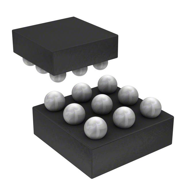
- Part No.:
- A21SP16J
- Manufacturer:
- STMicroelectronics
- Category:
- Audio Amplifiers
- Package:
- 9-UFBGA, FCBGA
- Datasheet:
-
 A21SP16J.pdf
- Description:
- IC AMP D MONO 1.4W 9FLIPCHIP
- Quantity:
- Payment:

- Shipping:

Inventory:23,730
Please send an inquiry. Send us your inquiry, and we will respond immediately.
Product details
Overview
A21SP16J from STMicroelectronics is a differential Class-D BTL audio power amplifier IC designed for ultra-low-power portable audio systems. It delivers 2.3 W into 4 Ω (1% THD+N, 5 V) and 1.4 W into 8 Ω (1% THD+N, 5 V), operates from 2.4–5.5 V, achieves 88% typical efficiency, and features active-low standby mode with 10 nA shutdown current - enabling use in wearable fitness trackers with battery life optimization.
For engineers reviewing the A21SP16J datasheet, A21SP16J pinout, A21SP16J application, or A21SP16J equivalent, key selection considerations include its flip-chip 9 × 300 µm package, differential input architecture, adjustable gain via external resistors, low pop/click noise (<5 ms wake-up), and thermal shutdown protection for compact, filter-free speaker drive.
Technical Context
The A21SP16J implements a PWM-based Class-D topology with a fixed 250 kHz base frequency and internal oscillator driving a full-bridge output stage. Its differential input structure includes common-mode feedback to stabilize DC offset and suppress supply ripple, achieving 63 dB PSRR at 217 Hz and 57 dB CMRR under standard conditions.
Gain is set externally using two matched resistors (Rin = 273–327 kΩ for 6 dB nominal), enabling precise control of signal path amplification without internal gain stages. The device integrates low-noise bias circuitry and pop/click suppression logic that ensures <5 ms wake-up time and controlled turn-on/turn-off transitions.
Key Specifications
| Parameter | Value and Actual Design Meaning |
|---|---|
| Output Power | 2.3 W @ 5 V into 4 Ω (1% THD+N); enables loud, clear audio from small speakers in space-constrained wearables |
| Supply Voltage Range | 2.4 V to 5.5 V; supports direct Li-ion/Li-poly battery operation without LDO pre-regulation |
| Efficiency | 88% typ. @ 2 W into 4 Ω; minimizes thermal dissipation and extends battery runtime in portable devices |
| Standby Current | 10 nA typ. @ GND-biased STBY pin; critical for multi-day battery life in always-on health monitors |
| THD+N | 0.4% max @ 1 W, 1 kHz, 8 Ω + 15 µH; meets fidelity requirements for voice and notification audio |
| SNR | 85 dB A-weighted @ 1.2 W into 8 Ω; ensures clean background for low-level audio playback |
| PWM Frequency | 250 kHz base frequency; allows use of small passive LC filters or filter-free operation with EMI-compliant layout |
| Wake-up Time | 5 ms max; enables responsive audio activation in gesture-triggered or sensor-wake applications |
Pinout & Package
Package: Lead-free flip-chip, 9 × 300 µm (0.009" × 0.030"), no external leads - requires micro-soldering or conductive adhesive assembly on PCB.
| Pin/Terminal | Circuit Role | Design Meaning |
|---|---|---|
| VDD (A1, C1, C2, C3) | Analog power supply | Four dedicated VDD pads for low-impedance power delivery and thermal spreading across flip-chip die |
| GND (B1, B3) | Power ground | Dual ground terminals minimize ground bounce and improve PSRR in high-frequency switching |
| IN+ / IN− (A2 / A3) | Differential audio input | High-CMRR input pair rejects noise in noisy portable environments; requires matched trace routing |
| STBY (B2) | Active-low standby control | Pulled low to enter 10 nA shutdown; open or high disables standby - no pull-up required |
| OUT+ / OUT− (B1 / B2) | Differential BTL output | Drives speaker directly in bridge-tied-load configuration; no DC-blocking capacitor needed |
Key Features
| Feature | Design Value |
|---|---|
| Filter-free operation | Enables direct speaker connection without external LC filter, reducing BOM count and PCB area by ≥3 components |
| Adjustable gain | 6 dB nominal gain set via external 300 kΩ resistor; scalable to ±3 dB via resistor tolerance selection |
| Low pop/click noise | Integrated soft-start and output mute sequencing limits audible transients during power cycling |
| Thermal shutdown | Auto-shutdown at 150 °C junction temperature; recovers automatically after cooling - protects speaker and PCB |
| Ultra-low standby current | 10 nA shutdown draw allows integration into energy-harvesting or coin-cell-powered edge nodes |
Applications
| Wearable Audio System | Fitness Tracker Audio Feedback |
|---|---|
Use Scenario: Compact earbud-style audio output in smart glasses or hearables with single-cell battery. IC Role / Device Role / Timing Role: Class-D BTL amplifier driving 8 Ω balanced armature driver with differential input rejecting RF-coupled noise. Use Value: 88% efficiency extends 120 mAh battery life to >8 hours continuous playback; 5 ms wake-up enables instant voice prompt response. | Use Scenario: Haptic-audio alerts in wrist-worn activity monitors during workout sessions. IC Role / Device Role / Timing Role: Low-power audio driver for short-duration beeps and spoken coaching cues triggered by motion sensors. Use Value: 10 nA standby current preserves battery over 14-day tracking cycles; 2.3 W peak power drives loud, intelligible alerts even in noisy gym environments. |
| Cellular Phone Speakerphone | PDA Voice Interface |
Use Scenario: Full-duplex speakerphone mode in slim smartphones with limited board space for audio subsystems. IC Role / Device Role / Timing Role: Differential-input Class-D amplifier eliminating need for AC-coupling capacitors and reducing component count. Use Value: Filter-free operation eliminates 2× 10 µF electrolytics and 2× 15 µH inductors; 63 dB PSRR maintains clarity during cellular transmit bursts. | Use Scenario: Voice-guided navigation and command feedback in handheld PDAs used in logistics or field service. IC Role / Device Role / Timing Role: Audio power stage interfacing with codec's differential output to drive mono speaker with minimal latency. Use Value: 2.4 V minimum supply enables operation down to end-of-life battery voltage; 85 dB SNR ensures speech intelligibility in warehouse ambient noise. |
Equivalent & Alternatives
The following parts are listed as comparable options for similar Class-D audio amplifier applications.
| Alternative Part | Technical Difference | Application Difference | Selection Advice |
|---|---|---|---|
| MAX98357AETE+T | I²S digital input; fixed 12 dB gain; requires external clock; no differential analog input | Suitable for SoC-connected designs with I²S output; not compatible with analog line-in or codec DAC outputs | Select when system uses digital audio interface and space permits 20-pin TQFN; avoid for analog-sensor-triggered audio paths |
| TAS5707PAG | 32-pin HTQFP; 3 W into 8 Ω @ 10% THD+N; integrated digital volume control; higher quiescent current (6 mA) | Better suited for mid-tier tablets with thermal margin; lacks ultra-low standby current for battery-critical wearables | Prefer for applications needing programmable EQ or multi-channel support; not optimal for sub-10 µA standby requirement |
Compared with MAX98357AETE+T and TAS5707PAG, the A21SP16J uniquely balances ultra-low standby current (10 nA), analog differential input flexibility, and flip-chip footprint - making it the only viable choice for space- and energy-constrained wearable audio where digital interfaces are unavailable or undesirable.
Availability
A21SP16J is available at Aetrix Electronics and suitable for wearable audio systems, fitness tracker feedback modules, and cellular phone speakerphone circuits requiring stable component supply across long-lifecycle consumer programs.
Supply support for A21SP16J includes scheduled delivery planning, volume procurement assistance, BOM continuity management, traceable sourcing, and lifecycle availability coordination for OEM customers, industrial embedded developers, connected-device designers, and electronics production programs.
Manufacturer
STMicroelectronics is a global semiconductor leader headquartered in Geneva, specializing in power management, analog, MEMS, and microcontrollers for industrial, automotive, and consumer markets.
The A21SP16J belongs to ST's ultra-low-power Class-D audio amplifier product line, engineered specifically for battery-operated portable devices demanding high efficiency, miniature packaging, and robust noise immunity in dense PCB layouts.
FAQ
What is the recommended PCB layout for minimizing EMI with the A21SP16J?
Place 1 µF ceramic bypass capacitor (Cs1) within 1 mm of each VDD pad and add 100 nF (Cs2) near the center VDD/GND pair. Route IN+/IN− differentially with 50 Ω controlled impedance and length matching ≤100 µm. Keep OUT+/OUT− traces symmetrical and avoid crossing noisy digital lines. Ground plane must be solid and unbroken beneath the flip-chip die area.
Can the A21SP16J drive an 8 Ω speaker without an LC filter?
Yes - the A21SP16J is specified for filter-free operation into 8 Ω loads. At 5 V supply, it delivers 1.4 W with 1% THD+N and meets EN 55032 Class B radiated emissions when PCB layout follows ST's footprint recommendations (e.g., minimized loop area, ground stitching vias every 3 mm around output traces).
How is gain adjusted, and what resistor tolerance is acceptable?
Gain is set by a single external resistor (Rin) tied between IN+ and IN−, with nominal value 300 kΩ for 6 dB. Gain = 300 kΩ / Rin (in kΩ). ±1% metal-film resistors are recommended; ±5% tolerance yields ±0.4 dB gain error, which remains within typical audio system calibration margins.
Does the A21SP16J require a startup delay circuit for system-level sequencing?
No - the A21SP16J has no power-on reset requirement. It enters functional state within 5 ms of STBY rising above 1.4 V (VCC threshold), and output is muted until internal bias stabilizes. No external RC delay or sequencer is needed; microcontroller GPIO can directly drive STBY after power rail stabilization.
A21SP16J Specifications
- Product attributes
- Attribute value
- Manufacturer:
- STMicroelectronics
- Series:
- -
- Package/Case:
- 9-UFBGA, FCBGA
- Packaging:
- Tape & Reel (TR)
- Product Status:
- Active
- Type:
- Class D
- Output Type:
- 1-Channel (Mono)
- Max Output Power x Channels @ Load:
- 1.4W x 1 @ 8Ohm
- Voltage - Supply:
- 2.4V ~ 5.5V
- Features:
- Depop, Thermal Protection
- Mounting Type:
- Surface Mount
- Operating Temperature:
- -40°C ~ 85°C (TA)
- Grade:
- -
- Qualification:
- -
- Supplier Device Package:
- 9-Flipchip (1.6x1.6)
A21SP16J FAQ
1.How can I place an order for A21SP16J through Aetrix?
Please submit a Request for Quotation (RFQ) for A21SP16J on Aetrix. Our sales agent will provide a competitive quotation and guide you through the order confirmation once you accept the terms.
2.Are the price and stock information for A21SP16J reliable?
The price and inventory of A21SP16J are updated periodically and may fluctuate due to market conditions. Stock and pricing data are typically refreshed every 24 hours. Quotation validity for A21SP16J is usually 5 days.
3.What payment methods are accepted for A21SP16J?
We accept Wire Transfer, PayPal, Credit Card, Western Union, MoneyGram, and Escrow for A21SP16J transactions.
Note: Certain payment methods may incur a processing fee.
4.How is shipping managed for A21SP16J?
A21SP16J orders can be shipped via leading logistics carriers, including DHL, UPS, FedEx, TNT, or Registered Mail.
Once your A21SP16J order is processed, you will receive an email with the shipment details and tracking number.
Note: Tracking information may take up to 24 hours to appear. Express delivery typically takes 3–5 business days.
5.How can I obtain technical support or documentation for A21SP16J?
For technical support, including A21SP16J datasheets, pinout diagrams, or application guidance, please contact our engineering support team. They can provide detailed documentation and assistance for your A21SP16J requirements.
6.How does Aetrix verify that A21SP16J is sourced from the original manufacturer or authorized distributors?
All A21SP16J products on Aetrix are procured from qualified distributors and authorized channels. Our dedicated quality assurance team conducts strict verification, including traceability checks and, if necessary, third-party testing. This ensures that A21SP16J meets industry standards.
7.What is the process for return or replacement of A21SP16J?
All A21SP16J units undergo pre-shipment inspection (PSI). If there is an issue with A21SP16J, returns or replacements are accepted under the following conditions:
1.Quantity discrepancies, incorrect items, or visible external defects (such as breakage or corrosion), acknowledged by Aetrix.
2.The issue is reported within 90 days of delivery.
3.The A21SP16J part is unused and in its original packaging.
Return procedure for A21SP16J:
1.Submit a request within 90 days.
2.Obtain a Return Material Authorization (RMA) from Aetrix.
A21SP16J Tags
-Exposed-Pad.jpg)
-
TS34119CS RLG
Taiwan Semiconductor Corporation

-
LM386MX-1/NOPB
Texas Instruments

-
TPA711DGNR
Texas Instruments

-
LM386N-4/NOPB
Texas Instruments

-
TS4990IST
STMicroelectronics
-
PAM8302AASCR
Diodes Incorporated
-
TPA6130A2RTJR
Texas Instruments
-
TPA6111A2DGNR
Texas Instruments
-
LM4861MX/NOPB
Texas Instruments
-
LM386M-1/NOPB
Texas Instruments

-
NCS2211DR2G
onsemi
-
IS31AP2005-DLS2-TR
Lumissil Microsystems
Tech Hub

A practical engineering and sourcing framework covering lifecycle verification, lifetime-buy calculations, replacement qualification, supplier checks and counterfeit-risk controls.

TTL and CMOS logic families differ in thresholds, loading, output drive, power and timing. This engineering guide compares 74HC and 74HCT, calculates noise margins and checks 3.3 V/5 V compatibility.

A practical engineering guide to 3.3V and 5V logic compatibility, input thresholds, resistor dividers, translator ICs, MOSFET level shifting, I2C pull-ups, timing limits and power-sequencing risks.

The 74HC595 uses push-pull logic outputs, while the TPIC6B595 uses 50 V open-drain DMOS sinks for higher-power loads. This guide compares timing, current limits, 3.3 V interfacing, load wiring, thermal…

The 74HC595 converts serial data into eight stable parallel outputs. This guide covers pin functions, shift and storage timing, OE and MR behavior, drive-current limits, cascading, voltage compatibilit…

A technical comparison of level-sensitive latches and edge-triggered flip-flops, covering timing windows, setup and hold limits, master–slave operation, time borrowing, race-through, HDL inference and…

A D latch stores one bit while Enable controls when data can pass. This reference covers gate-level operation, truth tables, transparency, setup and hold timing, LE versus OE, common ICs and practical …

An SR latch stores one bit through cross-coupled feedback. This engineering reference covers NOR and NAND implementations, truth tables, forbidden-state recovery, gated operation, switch debouncing, fa…

Latch circuits retain one bit through feedback. This technical reference covers SR and D latches, truth tables, transparency, timing limits, latch-versus-flip-flop behavior, applications and common log…

An engineering guide to LED driver operation, constant-current and constant-voltage outputs, linear and switching topologies, dimming, IC selection, calculations, replacement compatibility, and fault c…


