
 My Inquiry
 My Account


Allegro MicroSystems A4926KLPTR-T
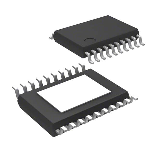
- Part No.:
- A4926KLPTR-T
- Manufacturer:
- Allegro MicroSystems
- Category:
- Gate Drivers
- Package:
- 20-TSSOP (0.173", 4.40mm Width) Exposed Pad
- Datasheet:
-
 A4926KLPTR-T.pdf
- Description:
- IC GATE DRVR HALF-BRIDGE 20TSSOP
- Quantity:
- Payment:

- Shipping:

Inventory:8,000
Please send an inquiry. Send us your inquiry, and we will respond immediately.
Product details
Overview
A4926KLPTR-T from Allegro MicroSystems is an automotive-grade N-channel half-bridge MOSFET driver designed for high-power inductive loads including brush DC motors, solenoids, and actuators. It operates from 5.5 V to 50 V, integrates a charge pump regulator enabling full gate drive down to 5.5 V, and supports SPI-compatible serial control with programmable dead time (0.1–3.15 µs) and VDS fault thresholds.
For engineers reviewing the A4926KLPTR-T datasheet, A4926KLPTR-T pinout, A4926KLPTR-T application, or A4926KLPTR-T equivalent, this device delivers ASIL B-compliant safety functionality, dual-control mode (logic inputs or SPI), integrated diagnostics with fault reporting via DIAG pin and serial interface, and thermal protection up to 180 °C transient junction temperature - critical for ABS, HVAC blower, and fuel pump designs.
Technical Context
The A4926KLPTR-T implements a dual-path control architecture: independent logic-level inputs (HS/LSn/ENABLE) and an SPI-compatible 16-bit serial interface for configuration and diagnostics. Its internal charge pump regulator generates either 8 V or 11 V (programmable via VRG bit) on VREG to power low-side drivers and bootstrap charging circuitry.
It features hardware-enforced shoot-through prevention via adjustable dead time, synchronous rectification support, and a bootstrap manager that actively recharges the C–S capacitor during high-duty-cycle PWM operation. Fault detection includes VDS monitoring (programmable 0–3.15 V threshold), overtemperature (170–180 °C trip), VREG undervoltage/overvoltage, and bootstrap undervoltage (56–64% of VREG).
Key Specifications
| Parameter | Value and Actual Design Meaning |
|---|---|
| Supply Voltage Range | 5.5 V to 50 V - enables direct connection to automotive battery rails with cold-crank tolerance down to 5.5 V |
| VREG Output Voltage | Programmable 8 V or 11 V - sets gate drive strength and determines bootstrap charging capability |
| Dead Time Range | 0.1 µs to 3.15 µs (default 1.6 µs) - prevents cross-conduction while supporting high-frequency PWM |
| Gate Drive Strength | High-side RDS(on) = 4–19 Ω (25–150 °C); Low-side RDS(on) = 1.5–5.5 Ω - ensures fast MOSFET switching with <200 ns turn-on/turn-off times |
| Diagnostic Coverage | VDS, overtemperature (170–180 °C), VREG UV/OV, bootstrap UV, and short-circuit detection - provides layered protection for safety-critical loads |
| Safety Certification | ASIL B hardware safety element out-of-context (SEooC) per ISO 26262 - validated for integration into automotive safety-related systems when used per safety manual |
| Operating Temperature | −40 °C to +150 °C ambient, 165 °C max continuous junction - qualified for under-hood automotive environments |
Pinout & Package
Supplied in a 20-lead eTSSOP package (6.5 mm × 4.4 mm, 1.2 mm max height) with exposed thermal pad (suffix LP), lead-free and 100% matte-tin plated.
| Pin/Terminal | Circuit Role | Design Meaning |
|---|---|---|
| GND (1) | Power, analog, and digital ground reference | Must be connected to system ground with low-impedance path; thermal pad (PAD) also tied to GND for heat dissipation |
| DIAG (2) | Open-drain diagnostic output | Asserts low for any latched fault (VDS, thermal, supply, bootstrap); active-low flag readable without SPI |
| ENABLE (3) | Gate drive enable control input | Battery-voltage compliant (0–50 V); disables GH/GL outputs when low; pull-down enabled |
| RESETn (4) | Active-low reset and sleep control | Pulse low ≥0.5 µs clears faults; held low >30 µs forces low-power sleep mode |
| HS (5) | High-side control input | Logic-level (TTL/CMOS) or battery-voltage compliant input; controls GH output directly when serial interface inactive |
| LSn (6) | Active-low low-side control input | Pull-up enabled; drives GL low when asserted; compatible with single-PWM or dual-PWM bridge control |
| SDI (7) | Serial data input (msb-first) | 16-bit command/data register write; pull-down enabled; accepts 3.3 V or 5 V logic |
| SCK (8) | Serial clock input | Rising-edge triggered; requires 16 edges per transfer; pull-down enabled |
| SDO (9) | Serial data output | Tri-state (high-Z when STRn high); outputs diagnostic register bit 15 (fault flag) immediately on STRn assertion |
| STRn (10) | Serial strobe / chip select | Active-low enable for serial interface; pull-up enabled; must be low for SCK/SDI activity |
| LSS (11) | Low-side source return | Independent low-impedance path to low-side MOSFET source - isolates gate discharge current from main GND |
| GL (12) | Low-side gate drive output | Drives external N-MOSFET gate; sourced from VREG; RDS(on) ≤ 3.1 Ω @ 25 °C |
| GH (13) | High-side gate drive output | Floating output referenced to S terminal; powered by bootstrap capacitor (C–S); RDS(on) ≤ 10.5 Ω @ 25 °C |
| S (14) | High-side source (load connection) | Bridge output node; connects to high-side MOSFET source and load; reference for GH drive |
| C (15) | Bootstrap supply terminal | Connects to positive side of bootstrap capacitor; supplies floating high-side driver; voltage = VBOOT ≈ VREG + VS |
| VREG (16) | Regulated gate drive supply | Programmable 8 V or 11 V output; powers GL, charge pump, and bootstrap manager; requires ≥10 µF ceramic storage cap |
| CP2 (17) | Charge pump capacitor connection | Paired with CP1; connects to 470 nF ceramic pump capacitor (CP1–CP2) for VREG boost regulation |
| CP1 (18) | Charge pump capacitor connection | Paired with CP2; forms resonant tank with internal charge pump switch for VREG generation |
| VBB (19) | Main power supply input | 5.5–50 V unregulated input; powers internal regulators, logic, and charge pump; decouple with 100 nF ceramic near pin |
| VBRG (20) | High-side drain voltage sense | Monitors VDS of high-side MOSFET; enables programmable short-circuit detection (0–3.15 V threshold) |
Key Features
| Feature | Design Value |
|---|---|
| ASIL B SEooC compliance | Hardware safety element developed per ISO 26262 for integration into automotive safety systems - eliminates need for redundant external safety monitors |
| Programmable dead time | Adjustable 0.1–3.15 µs via SPI register DT[5:0] - balances shoot-through risk against conduction loss in motor control |
| Bootstrap manager | Automatic recharge of C–S capacitor during high-duty-cycle PWM - prevents bootstrap undervoltage faults without processor intervention |
| Dual control interface | Direct logic inputs (HS/LSn) OR SPI serial interface - enables simple legacy integration or advanced configurability and diagnostics |
| VDS fault monitoring | Configurable high- and low-side VDS thresholds (0–3.15 V) with blank/debounce timing - detects open-load, short-to-battery, and short-to-ground conditions |
| Top-off charge pump | Low-current trickle charge maintains high-side gate voltage indefinitely - enables true 100% duty cycle operation without gate droop |
Applications
| Anti-lock Braking Systems (ABS) | HVAC Blower Fan Control |
|---|---|
Use Scenario: Precise modulation of solenoid valves in hydraulic brake circuits during emergency braking events. IC Role / Device Role / Timing Role: Half-bridge driver controlling N-MOSFETs in valve actuator power stage; delivers fast, robust gate drive under 12 V battery sag. Use Value: ASIL B compliance ensures functional safety integrity; programmable dead time prevents shoot-through during rapid PWM transitions required for pressure modulation. | Use Scenario: Variable-speed control of 24 V DC blower motors in automotive climate systems. IC Role / Device Role / Timing Role: High-efficiency half-bridge pre-driver enabling synchronous rectification and regenerative braking capability. Use Value: Bootstrap manager sustains gate drive at >95% duty cycle; integrated VDS diagnostics detect motor stall or wiring faults before thermal damage occurs. |
| Fuel/Oil/Water Pump Control | Solenoid & Linear Actuator Drive |
Use Scenario: Continuous-duty driving of 48 V brush DC fuel pumps in start-stop and hybrid powertrains. IC Role / Device Role / Timing Role: Robust gate driver interfacing with discrete N-MOSFETs; handles wide input range (5.5–50 V) and harsh EMI environments. Use Value: Charge pump regulator maintains 11 V gate drive down to 7 V VBB; thermal shutdown (175 °C) protects against pump seizure-induced overheating. | Use Scenario: Fast-acting linear motion control for transmission shift solenoids or throttle actuators. IC Role / Device Role / Timing Role: Precision half-bridge controller delivering microsecond-level dead time control and accurate VDS-based current limiting. Use Value: Programmable VDS threshold (1.1–3.15 V) enables precise short-circuit detection across varying solenoid coil resistances and temperatures. |
Equivalent & Alternatives
The following parts are listed as comparable options for similar half-bridge MOSFET driver applications.
| Alternative Part | Technical Difference | Application Difference | Selection Advice |
|---|---|---|---|
| TLE9201SG | Integrated high-/low-side drivers with embedded current sense; fixed 1.5 µs dead time; no SPI interface; 5–28 V operating range | Targeted at cost-sensitive 12 V automotive loads; lacks programmable diagnostics and ASIL B SEooC certification | Select TLE9201SG only for non-safety-critical 12 V solenoid control where SPI configurability and extended voltage range are unnecessary |
| MPQ6532-AEC1 | Automotive-qualified half-bridge driver with 5–36 V range; SPI interface; ASIL B compliance; but no bootstrap manager or VDS monitoring | Designed for brushed DC motor control with integrated current regulation; lacks high-side drain sensing for short-circuit localization | Choose MPQ6532-AEC1 when current regulation and compact footprint outweigh need for VDS-based fault discrimination and bootstrap autonomy |
Compared with TLE9201SG and MPQ6532-AEC1, the A4926KLPTR-T uniquely combines ASIL B SEooC certification, programmable VDS monitoring with blank/debounce modes, and autonomous bootstrap management - making it the only option qualified for safety-critical 5.5–50 V inductive load control requiring field-configurable fault response.
Availability
A4926KLPTR-T is available at Aetrix Electronics and suitable for anti-lock braking systems (ABS), HVAC blower fan control, and fuel/oil/water pump applications requiring stable component supply across automotive production lifecycles.
Supply support for A4926KLPTR-T includes scheduled delivery planning, volume procurement assistance, BOM continuity management, traceable sourcing, and lifecycle availability coordination for OEM customers, industrial embedded developers, connected-device designers, and electronics production programs.
Manufacturer
Allegro MicroSystems is a U.S.-based designer and manufacturer of high-performance magnetic sensors and power ICs, specializing in automotive and industrial motion control solutions.
The A4926 product line delivers robust, safety-certified half-bridge drivers for high-power inductive loads - engineered specifically for automotive subsystems demanding functional safety, wide input voltage tolerance, and intelligent diagnostics.
FAQ
What is the minimum supply voltage required for full gate drive operation of the A4926KLPTR-T?
The A4926KLPTR-T guarantees full gate drive (8 V or 11 V on VREG) down to 5.5 V VBB when the charge pump regulator is active. At 7–50 V, it delivers nominal VREG; below 7 V, gate drive voltage is reduced but functional operation is maintained - critical for cold-crank automotive conditions. This behavior is confirmed in the Electrical Characteristics table under "VREG Output Voltage" test conditions.
How does the A4926KLPTR-T prevent shoot-through in the external MOSFET half-bridge?
The A4926KLPTR-T prevents shoot-through using two complementary mechanisms: a programmable hardware dead time (0.1–3.15 µs) inserted between high-side turn-off and low-side turn-on (and vice versa), plus a hardwired logic lockout that physically blocks simultaneous GH/GL activation. These features are implemented in silicon and operate independently of software or SPI configuration - ensuring deterministic protection even during fault conditions.
Can the A4926KLPTR-T be used without the SPI interface?
Yes, the A4926KLPTR-T supports fully independent logic-level control via HS, LSn, ENABLE, and RESETn pins - no SPI interface required. The device defaults to logic-input mode at power-up; SPI is optional for advanced configuration (dead time, VDS thresholds, fault blanking) and diagnostic readback. All safety-critical protections (thermal, VREG UV/OV, bootstrap UV) remain fully active in logic-only mode.
What is the purpose of the VBRG pin on the A4926KLPTR-T?
The VBRG pin on the A4926KLPTR-T senses the drain voltage of the external high-side MOSFET, enabling real-time VDS monitoring for short-circuit and open-load detection. It supports programmable fault thresholds (0–3.15 V) and configurable blank/debounce timing (0–6.3 µs). This allows precise discrimination between normal switching transients and actual overcurrent events - a key enabler for ASIL B-compliant fault handling in motor and solenoid applications.
Does the A4926KLPTR-T require external bootstrap diodes or capacitors?
No, the A4926KLPTR-T integrates a bootstrap diode (forward voltage 0.4–1.0 V at 10 mA) and requires only an external ceramic bootstrap capacitor (typically 1–10 µF) between C and S pins. The internal diode eliminates need for discrete components, reducing BOM count and PCB area. The bootstrap manager automatically recharges this capacitor during operation - eliminating reliance on external timing or processor intervention for sustained high-duty-cycle use.
A4926KLPTR-T Specifications
- Product attributes
- Attribute value
- Manufacturer:
- Allegro MicroSystems
- Series:
- -
- Package/Case:
- 20-TSSOP (0.173", 4.40mm Width) Exposed Pad
- Packaging:
- Tape & Reel (TR)
- Product Status:
- Active
- Programmable:
- Not Verified
- Driven Configuration:
- Half-Bridge
- Channel Type:
- Independent
- Number of Drivers:
- 2
- Gate Type:
- N-Channel MOSFET
- Voltage - Supply:
- 5.5V ~ 50V
- Logic Voltage - VIL, VIH:
- 0.8V, 2V
- Current - Peak Output (Source, Sink):
- -
- Input Type:
- Non-Inverting
- High Side Voltage - Max (Bootstrap):
- -
- Rise / Fall Time (Typ):
- -
- Operating Temperature:
- -40°C ~ 150°C (TJ)
- Grade:
- -
- Qualification:
- -
- Mounting Type:
- Surface Mount
- Supplier Device Package:
- 20-TSSOP-EP
A4926KLPTR-T FAQ
1.How can I place an order for A4926KLPTR-T through Aetrix?
Please submit a Request for Quotation (RFQ) for A4926KLPTR-T on Aetrix. Our sales agent will provide a competitive quotation and guide you through the order confirmation once you accept the terms.
2.Are the price and stock information for A4926KLPTR-T reliable?
The price and inventory of A4926KLPTR-T are updated periodically and may fluctuate due to market conditions. Stock and pricing data are typically refreshed every 24 hours. Quotation validity for A4926KLPTR-T is usually 5 days.
3.What payment methods are accepted for A4926KLPTR-T?
We accept Wire Transfer, PayPal, Credit Card, Western Union, MoneyGram, and Escrow for A4926KLPTR-T transactions.
Note: Certain payment methods may incur a processing fee.
4.How is shipping managed for A4926KLPTR-T?
A4926KLPTR-T orders can be shipped via leading logistics carriers, including DHL, UPS, FedEx, TNT, or Registered Mail.
Once your A4926KLPTR-T order is processed, you will receive an email with the shipment details and tracking number.
Note: Tracking information may take up to 24 hours to appear. Express delivery typically takes 3–5 business days.
5.How can I obtain technical support or documentation for A4926KLPTR-T?
For technical support, including A4926KLPTR-T datasheets, pinout diagrams, or application guidance, please contact our engineering support team. They can provide detailed documentation and assistance for your A4926KLPTR-T requirements.
6.How does Aetrix verify that A4926KLPTR-T is sourced from the original manufacturer or authorized distributors?
All A4926KLPTR-T products on Aetrix are procured from qualified distributors and authorized channels. Our dedicated quality assurance team conducts strict verification, including traceability checks and, if necessary, third-party testing. This ensures that A4926KLPTR-T meets industry standards.
7.What is the process for return or replacement of A4926KLPTR-T?
All A4926KLPTR-T units undergo pre-shipment inspection (PSI). If there is an issue with A4926KLPTR-T, returns or replacements are accepted under the following conditions:
1.Quantity discrepancies, incorrect items, or visible external defects (such as breakage or corrosion), acknowledged by Aetrix.
2.The issue is reported within 90 days of delivery.
3.The A4926KLPTR-T part is unused and in its original packaging.
Return procedure for A4926KLPTR-T:
1.Submit a request within 90 days.
2.Obtain a Return Material Authorization (RMA) from Aetrix.
A4926KLPTR-T Tags

-
ZXGD3009E6TA
Diodes Incorporated
-
1EDN7512BXTSA1
Infineon Technologies

-
UCC27517DBVR
Texas Instruments

-
MCP1416T-E/OT
Microchip Technology
-
MCP1402T-E/OT
Microchip Technology
-
MCP1415T-E/OT
Microchip Technology
-
MCP1401T-E/OT
Microchip Technology
-
IX4428NTR
Littelfuse Inc.

-
IRS2005STRPBF
Infineon Technologies
-
IRS2008STRPBF
Infineon Technologies
-
IX4310TTR
Littelfuse Inc.

-
2EDN7524RXTMA1
Infineon Technologies
Tech Hub

A practical engineering and sourcing framework covering lifecycle verification, lifetime-buy calculations, replacement qualification, supplier checks and counterfeit-risk controls.

TTL and CMOS logic families differ in thresholds, loading, output drive, power and timing. This engineering guide compares 74HC and 74HCT, calculates noise margins and checks 3.3 V/5 V compatibility.

A practical engineering guide to 3.3V and 5V logic compatibility, input thresholds, resistor dividers, translator ICs, MOSFET level shifting, I2C pull-ups, timing limits and power-sequencing risks.

The 74HC595 uses push-pull logic outputs, while the TPIC6B595 uses 50 V open-drain DMOS sinks for higher-power loads. This guide compares timing, current limits, 3.3 V interfacing, load wiring, thermal…

The 74HC595 converts serial data into eight stable parallel outputs. This guide covers pin functions, shift and storage timing, OE and MR behavior, drive-current limits, cascading, voltage compatibilit…

A technical comparison of level-sensitive latches and edge-triggered flip-flops, covering timing windows, setup and hold limits, master–slave operation, time borrowing, race-through, HDL inference and…

A D latch stores one bit while Enable controls when data can pass. This reference covers gate-level operation, truth tables, transparency, setup and hold timing, LE versus OE, common ICs and practical …

An SR latch stores one bit through cross-coupled feedback. This engineering reference covers NOR and NAND implementations, truth tables, forbidden-state recovery, gated operation, switch debouncing, fa…

Latch circuits retain one bit through feedback. This technical reference covers SR and D latches, truth tables, transparency, timing limits, latch-versus-flip-flop behavior, applications and common log…

An engineering guide to LED driver operation, constant-current and constant-voltage outputs, linear and switching topologies, dimming, IC selection, calculations, replacement compatibility, and fault c…


