
 My Inquiry
 My Account


Allegro MicroSystems A6862KLPTR-T
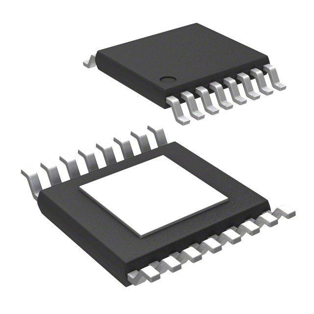
- Part No.:
- A6862KLPTR-T
- Manufacturer:
- Allegro MicroSystems
- Category:
- Gate Drivers
- Package:
- 16-TSSOP (0.173", 4.40mm Width) Exposed Pad
- Datasheet:
-
 A6862KLPTR-T.pdf
- Description:
- IC GATE DRVR HIGH-SIDE 16TSSOP
- Quantity:
- Payment:

- Shipping:

Inventory:7,735
Please send an inquiry. Send us your inquiry, and we will respond immediately.
Product details
Overview
A6862KLPTR-T from Allegro MicroSystems is an automotive-grade 3-phase N-channel MOSFET driver IC designed for phase-isolated solid-state relay applications in high-reliability systems. It delivers three independent floating gate drives, operates across 4.5–50 V supply range, maintains >7.5 V gate drive down to 4.5 V battery voltage with 100 kΩ gate-source resistors, and switches MOSFETs on in ≤8 µs and off in ≤1 µs-enabling robust electric power steering (EPS) and ASIL D-compliant 3-phase disconnect functions.
For engineers reviewing the A6862KLPTR-T datasheet, A6862KLPTR-T pinout, A6862KLPTR-T application, or A6862KLPTR-T equivalent, key selection criteria include its integrated charge pump architecture, VCP/VGS undervoltage monitoring, dual activation inputs (IG/POK), thermal performance up to 150°C ambient, and TSSOP-16 LP package with exposed pad for automotive motor control isolation.
Technical Context
The A6862KLPTR-T implements a regulated charge pump topology that generates VCP ≥7.5 V above VBB to sustain N-channel MOSFET conduction during high dv/dt phase transients-even when source voltage equals battery voltage. Its three floating gate drivers (GU/GV/GW) reference respective phase sources (SU/SV/SW), enabling true phase-isolation without shared ground constraints.
Control logic integrates dual activation inputs (IG and POK) requiring simultaneous high states to enable the charge pump; ENA serves as both phase-enable input and open-drain fault indicator output. Undervoltage protection monitors both VCP (threshold 6.5–7.5 V w.r.t. VBB) and individual VGSx (6.0–7.0 V), with programmable filter times (tCPUV = 12.5 µs, tGSUV = 3.7–18 µs) to reject transient noise while ensuring safe MOSFET conduction.
Key Specifications
| Parameter | Value and Actual Design Meaning |
|---|---|
| VBB Operating Range | 4.5–50 V - supports full automotive battery range including cold-crank (4.5 V) and load-dump (50 V) conditions without undefined states. |
| VCP Output Voltage | 7.5–11 V w.r.t. VBB - regulates above-battery voltage to ensure full enhancement of external N-MOSFETs even at low VBB. |
| Gate Drive Turn-On/Off Time | ≤8 µs / ≤1 µs - enables fast, deterministic switching for safety-critical EPS and braking actuation. |
| VGS Undervoltage Threshold | 6.0–7.0 V - guarantees MOSFET remains in safe conducting state; hysteresis of 200 mV prevents chatter during marginal conditions. |
| Thermal Resistance RθJA | 34 °C/W (4-layer PCB) - enables 150°C ambient operation with appropriate layout and thermal vias under typical EPS power dissipation. |
| Logic Input Voltage Tolerance | 0–50 V - all logic inputs (ENA, IG, POK) withstand battery rail directly, eliminating need for level-shifting in harsh automotive environments. |
| Supply Current (Active) | 11 mA typ. @ VBB = 12 V - balances drive capability with low quiescent consumption for always-on vehicle subsystems. |
Pinout & Package
Package: 16-lead TSSOP (LP) with exposed thermal pad (4.4 mm × 5.0 mm case); lead-free, 100% matte-tin plating; JEDEC MO-153 ABT compliant.
| Pin/Terminal | Circuit Role | Design Meaning |
|---|---|---|
| VBB (1) | Main power supply input | Accepts reverse-polarity protected 4.5–50 V battery rail; powers internal circuitry and charge pump base. |
| CP4 (2), CP3 (3), CP2 (4), CP1 (5) | Charge pump capacitor connections | Four terminals for two 330 nF ceramic pump capacitors (CP1–CP2 and CP3–CP4); critical for stable VCP generation at low VBB. |
| IG (6), POK (7) | Charge pump activation inputs | Independent logic-level inputs; both must be high to enable pump; tolerate 0–50 V, enabling direct battery or logic-supply connection. |
| ENA (8) | Phase-enable input / fault indicator output | Single logic signal controls all three gate drives; also functions as open-drain output pulled to VOLF (≤1.1 V) during VCP or VGS undervoltage. |
| GND (9) | Power ground reference | Main return path; exposed thermal pad must be connected to GND for thermal and electrical integrity. |
| SW (10), GV (13), GW (11), SU (14), SV (12), GU (15) | Phase source and gate drive outputs | Three matched pairs (SU/GU, SV/GV, SW/GW) provide floating gate drive referenced to respective motor phase sources-enabling true galvanic isolation per phase. |
| VCP (16) | Regulated pumped supply output | Provides 7.5–11 V above VBB; powers gate drives and can drive external reverse-battery protection MOSFETs; requires 1 µF decoupling to VBB. |
Key Features
| Feature | Design Value |
|---|---|
| Integrated charge pump regulator | Generates stable VCP ≥7.5 V above VBB down to 4.5 V input-eliminates need for external high-side gate drivers or bootstrap circuits in 3-phase isolation. |
| Floating gate drive architecture | Three independent GU/GV/GW outputs referenced to SU/SV/SW-supports source-connected MOSFET topologies essential for ASIL D-compliant phase disconnect. |
| Dual activation control (IG + POK) | Enables fail-safe pump disable: either input low forces sleep mode with <10 µA supply current-critical for system-level power management and fault containment. |
| VCP and VGS undervoltage monitoring | Dual independent monitors with programmable filter times (tCPUV = 12.5 µs, tGSUV = 3.7–18 µs) prevent false trips while guaranteeing MOSFET remains fully enhanced during transients. |
| Automotive-qualified thermal design | RθJA = 34 °C/W (4-layer PCB) and 150°C ambient rating-validated for under-hood EPS and braking modules with sustained high-power operation. |
| Battery-rail tolerant logic inputs | All digital pins (ENA, IG, POK) rated 0–50 V-allows direct connection to battery or logic rails without external clamping or level shifters, reducing BOM count and failure modes. |
Applications
| Electric Power Steering (EPS) | ASIL D 3-Phase Disconnect |
|---|---|
|
Use Scenario: Isolating 3-phase BLDC motor phases during EPS ECU reset or fault conditions to prevent unintended torque generation. IC Role / Device Role / Timing Role: A6862KLPTR-T acts as phase-isolation gate driver, controlling external N-MOSFETs to break motor phase continuity within ≤8 µs turn-on and ≤1 µs turn-off windows. Use Value: Enables deterministic, fail-safe motor disconnection meeting ISO 26262 ASIL D requirements-no reliance on microcontroller timing or software intervention. |
Use Scenario: Providing redundant 3-phase isolation in battery disconnect units for xEV traction inverters or high-voltage auxiliary systems. IC Role / Device Role / Timing Role: A6862KLPTR-T drives isolated N-MOSFETs per phase, using VCP-regulated gate drive and dual VGS monitoring to maintain safe conduction state under battery transients. Use Value: Achieves hardware-enforced phase isolation with built-in diagnostics-reducing system-level validation burden and eliminating single-point failure paths. |
| Electric Braking Actuation | 3-Phase Solid-State Relay Driver |
|
Use Scenario: Controlling brake caliper motor phases in electromechanical brake (EMB) systems where rapid, reliable isolation is required during emergency stops. IC Role / Device Role / Timing Role: A6862KLPTR-T provides synchronized gate drive to three N-MOSFETs per phase, with ENA-driven enable/disable and VCP fault reporting to brake ECU. Use Value: Guarantees sub-10 µs response time and continuous gate bias during high dv/dt braking transients-ensuring mechanical brake engagement integrity. |
Use Scenario: Replacing mechanical relays in industrial HVAC or energy storage systems requiring silent, wear-free 3-phase AC/DC load switching. IC Role / Device Role / Timing Role: A6862KLPTR-T serves as core gate driver for external N-MOSFETs configured as solid-state relays, leveraging charge pump for zero-crossing–independent turn-on. Use Value: Delivers >10⁶ cycle lifetime, no contact bounce, and immunity to vibration-while maintaining low RDS(on) via regulated >7.5 V gate drive across full 4.5–50 V input range. |
Equivalent & Alternatives
The following parts are listed as comparable options for similar 3-phase isolated MOSFET driver applications.
| Alternative Part | Technical Difference | Application Difference | Selection Advice |
|---|---|---|---|
| STGD18N40LZ | Discrete N-channel MOSFET (not a driver IC); lacks integrated charge pump, floating gate architecture, or VGS monitoring. | Requires external gate driver, level shifter, and protection circuitry-increasing board area and BOM complexity for phase-isolation use cases. | Select only if discrete implementation with custom gate drive is preferred; not drop-in compatible with A6862KLPTR-T functionality. |
| Infineon BTS7200-2EPA | High-side smart switch (single-channel, 40 V); no floating gate outputs, no charge pump, no multi-phase coordination. | Designed for load driving-not phase isolation; limited to unidirectional current flow and lacks VCP/VGS fault reporting. | Use only for non-isolated, single-phase high-side switching; cannot replicate A6862KLPTR-T's 3-phase floating drive or ASIL D diagnostic coverage. |
Compared with STGD18N40LZ and BTS7200-2EPA, the A6862KLPTR-T uniquely integrates charge-pump–based floating gate drive, dual activation control, and concurrent VCP/VGS monitoring-making it the only solution capable of hardware-enforced, self-diagnosing 3-phase isolation in automotive safety-critical systems without external support components.
Availability
A6862KLPTR-T is available at Aetrix Electronics and suitable for electric power steering (EPS), ASIL D 3-phase disconnect, and electric braking actuation requiring stable component supply, automotive qualification, and long-term lifecycle support.
Supply support for A6862KLPTR-T includes scheduled delivery planning, volume procurement assistance, BOM continuity management, traceable sourcing, and lifecycle availability coordination for OEM customers, industrial embedded developers, connected-device designers, and electronics production programs.
Manufacturer
Allegro MicroSystems is a U.S.-based designer and manufacturer of high-performance magnetic sensing and power IC solutions, specializing in automotive and industrial motion control.
The A6862KLPTR-T belongs to Allegro's automotive 3-phase isolator MOSFET driver product line, engineered specifically for hardware-level phase isolation in safety-critical electric vehicle subsystems such as EPS, braking, and battery management.
FAQ
What is the minimum VBB voltage required for A6862KLPTR-T to maintain functional gate drive?
The A6862KLPTR-T maintains functional gate drive down to VBB = 4.5 V, delivering >7.5 V gate-to-source voltage (VGS) with 100 kΩ gate-source resistors. Below 4.5 V, the device remains operational but does not guarantee VGS compliance; it sustains defined behavior down to 4.0 V for off-state retention and down to 0 V for deterministic power-up/power-down sequencing. This ensures robust cold-crank performance in automotive EPS and braking systems.
How does the A6862KLPTR-T implement phase isolation without shared ground references?
The A6862KLPTR-T achieves true phase isolation through three independent floating gate drive channels (GU/GV/GW), each referenced to its own phase source terminal (SU/SV/SW). Unlike conventional drivers tied to a common ground, this architecture allows each MOSFET to operate with source potentials differing by hundreds of volts-essential for ASIL D-compliant 3-phase disconnect where galvanic separation between phases must be maintained during faults or transients.
Can the A6862KLPTR-T drive MOSFETs with gate charges exceeding 400 nC?
Yes, the A6862KLPTR-T can drive MOSFETs with gate charge >400 nC, but requires larger external charge pump capacitors. The datasheet specifies that for total gate charge above 400 nC, both the VCP-to-VBB decoupling capacitor (CVCP) and pump capacitors (CP1–CP2, CP3–CP4) should be increased beyond the standard 1 µF and 330 nF values respectively-ensuring sufficient charge transfer during low-VBB operation and high-slew-rate phase switching.
What happens to the A6862KLPTR-T outputs when either IG or POK is pulled low?
When either IG or POK is pulled low, the A6862KLPTR-T disables its charge pump regulator, causing VCP to decay to zero. All gate drive outputs (GU/GV/GW) switch off, and the device enters a low-power sleep mode drawing ≤10 µA. This dual-input architecture provides hardware-level fault containment-preventing unintended MOSFET conduction during supply failures or system-level shutdown sequences.
How is fault status reported on the ENA pin of the A6862KLPTR-T?
The ENA pin of the A6862KLPTR-T serves as a bidirectional fault indicator: when no VCP or VGS undervoltage faults are present, ENA follows the externally applied logic signal; when either fault occurs, an internal open-drain transistor pulls ENA to VOLF (≤1.1 V at 10–500 µA), signaling fault presence to the host MCU. This enables three-state detection (ON/FAULT/OFF) using a single pull-up resistor and MCU GPIO-without requiring additional diagnostic lines.
A6862KLPTR-T Specifications
- Product attributes
- Attribute value
- Manufacturer:
- Allegro MicroSystems
- Series:
- -
- Package/Case:
- 16-TSSOP (0.173", 4.40mm Width) Exposed Pad
- Packaging:
- Tape & Reel (TR)
- Product Status:
- Active
- Programmable:
- Not Verified
- Driven Configuration:
- Floating
- Channel Type:
- 3-Phase
- Number of Drivers:
- 3
- Gate Type:
- N-Channel MOSFET
- Voltage - Supply:
- 4.5V ~ 50V
- Logic Voltage - VIL, VIH:
- 0.4V, 0.7V
- Current - Peak Output (Source, Sink):
- -
- Input Type:
- Non-Inverting
- High Side Voltage - Max (Bootstrap):
- -
- Rise / Fall Time (Typ):
- -
- Operating Temperature:
- -40°C ~ 150°C (TJ)
- Grade:
- -
- Qualification:
- -
- Mounting Type:
- Surface Mount
- Supplier Device Package:
- 16-eTSSOP-EP
A6862KLPTR-T FAQ
1.How can I place an order for A6862KLPTR-T through Aetrix?
Please submit a Request for Quotation (RFQ) for A6862KLPTR-T on Aetrix. Our sales agent will provide a competitive quotation and guide you through the order confirmation once you accept the terms.
2.Are the price and stock information for A6862KLPTR-T reliable?
The price and inventory of A6862KLPTR-T are updated periodically and may fluctuate due to market conditions. Stock and pricing data are typically refreshed every 24 hours. Quotation validity for A6862KLPTR-T is usually 5 days.
3.What payment methods are accepted for A6862KLPTR-T?
We accept Wire Transfer, PayPal, Credit Card, Western Union, MoneyGram, and Escrow for A6862KLPTR-T transactions.
Note: Certain payment methods may incur a processing fee.
4.How is shipping managed for A6862KLPTR-T?
A6862KLPTR-T orders can be shipped via leading logistics carriers, including DHL, UPS, FedEx, TNT, or Registered Mail.
Once your A6862KLPTR-T order is processed, you will receive an email with the shipment details and tracking number.
Note: Tracking information may take up to 24 hours to appear. Express delivery typically takes 3–5 business days.
5.How can I obtain technical support or documentation for A6862KLPTR-T?
For technical support, including A6862KLPTR-T datasheets, pinout diagrams, or application guidance, please contact our engineering support team. They can provide detailed documentation and assistance for your A6862KLPTR-T requirements.
6.How does Aetrix verify that A6862KLPTR-T is sourced from the original manufacturer or authorized distributors?
All A6862KLPTR-T products on Aetrix are procured from qualified distributors and authorized channels. Our dedicated quality assurance team conducts strict verification, including traceability checks and, if necessary, third-party testing. This ensures that A6862KLPTR-T meets industry standards.
7.What is the process for return or replacement of A6862KLPTR-T?
All A6862KLPTR-T units undergo pre-shipment inspection (PSI). If there is an issue with A6862KLPTR-T, returns or replacements are accepted under the following conditions:
1.Quantity discrepancies, incorrect items, or visible external defects (such as breakage or corrosion), acknowledged by Aetrix.
2.The issue is reported within 90 days of delivery.
3.The A6862KLPTR-T part is unused and in its original packaging.
Return procedure for A6862KLPTR-T:
1.Submit a request within 90 days.
2.Obtain a Return Material Authorization (RMA) from Aetrix.
A6862KLPTR-T Tags

-
ZXGD3009E6TA
Diodes Incorporated
-
1EDN7512BXTSA1
Infineon Technologies

-
UCC27517DBVR
Texas Instruments

-
MCP1416T-E/OT
Microchip Technology
-
MCP1402T-E/OT
Microchip Technology
-
MCP1415T-E/OT
Microchip Technology
-
MCP1401T-E/OT
Microchip Technology
-
IX4428NTR
Littelfuse Inc.

-
IRS2005STRPBF
Infineon Technologies
-
IRS2008STRPBF
Infineon Technologies
-
IX4310TTR
Littelfuse Inc.

-
2EDN7524RXTMA1
Infineon Technologies
Tech Hub

A practical engineering and sourcing framework covering lifecycle verification, lifetime-buy calculations, replacement qualification, supplier checks and counterfeit-risk controls.

TTL and CMOS logic families differ in thresholds, loading, output drive, power and timing. This engineering guide compares 74HC and 74HCT, calculates noise margins and checks 3.3 V/5 V compatibility.

A practical engineering guide to 3.3V and 5V logic compatibility, input thresholds, resistor dividers, translator ICs, MOSFET level shifting, I2C pull-ups, timing limits and power-sequencing risks.

The 74HC595 uses push-pull logic outputs, while the TPIC6B595 uses 50 V open-drain DMOS sinks for higher-power loads. This guide compares timing, current limits, 3.3 V interfacing, load wiring, thermal…

The 74HC595 converts serial data into eight stable parallel outputs. This guide covers pin functions, shift and storage timing, OE and MR behavior, drive-current limits, cascading, voltage compatibilit…

A technical comparison of level-sensitive latches and edge-triggered flip-flops, covering timing windows, setup and hold limits, master–slave operation, time borrowing, race-through, HDL inference and…

A D latch stores one bit while Enable controls when data can pass. This reference covers gate-level operation, truth tables, transparency, setup and hold timing, LE versus OE, common ICs and practical …

An SR latch stores one bit through cross-coupled feedback. This engineering reference covers NOR and NAND implementations, truth tables, forbidden-state recovery, gated operation, switch debouncing, fa…

Latch circuits retain one bit through feedback. This technical reference covers SR and D latches, truth tables, transparency, timing limits, latch-versus-flip-flop behavior, applications and common log…

An engineering guide to LED driver operation, constant-current and constant-voltage outputs, linear and switching topologies, dimming, IC selection, calculations, replacement compatibility, and fault c…


