
 My Inquiry
 My Account


NXP Semiconductors A7002CGHN1/T1AG502
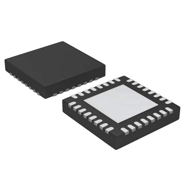
- Part No.:
- A7002CGHN1/T1AG502
- Manufacturer:
- NXP Semiconductors
- Category:
- Application Specific Microcontrollers
- Package:
- 32-VFQFN Exposed Pad
- Datasheet:
-
 A7002CGHN1/T1AG502.pdf
- Description:
- SECURE AUTHENTICATION MICROCONTR
- Quantity:
- Payment:

- Shipping:

Inventory:2,326
Please send an inquiry. Send us your inquiry, and we will respond immediately.
Product details
Overview
A7002CGHN1/T1AG502 from NXP Semiconductors is a tamper-resistant secure authentication microcontroller featuring the dedicated security-hardened MX51 CPU, 76.4 kB EEPROM, I²C slave interface (100 kbit/s), and JCOP 2.4.2 R1 Java Card OS. It operates across −40 °C to +90 °C and integrates hardware-accelerated cryptographic coprocessors for RSA-2048, ECC-320, AES-128/192/256, and triple-DES - deployed in e-passports, secure mobile identity, and embedded M2M authentication systems.
For engineers reviewing the A7002CGHN1/T1AG502 datasheet, A7002CGHN1/T1AG502 pinout, A7002CGHN1/T1AG502 application, or A7002CGHN1/T1AG502 equivalent, this page delivers verified electrical specs, package mapping, security architecture context, and real-world integration guidance for high-assurance embedded authentication design.
Technical Context
The A7002CGHN1/T1AG502 implements an asynchronous self-timed handshake architecture to resist timing-based side-channel attacks and integrates Secure Fetch Technology to protect ROM/RAM/EEPROM code fetches against laser and light fault injection. Its security stack includes active shielding, NXP glue logic, and >100 countermeasures validated under Common Criteria.
It executes JCOP 2.4.2 R1 compliant with Java Card 3.0.1 Classic and GlobalPlatform 2.1.1, supporting X.509 client authentication applets pre-installed in ROM. The device uses a 62 MHz internally generated CPU clock and supports wake-up from sleep mode via I²C communication - enabling low-power always-on secure identity in battery-constrained endpoints.
Key Specifications
| Parameter | Value and Actual Design Meaning |
|---|---|
| Core Architecture | MX51 security-hardened 80C51 derivative with asynchronous handshaking circuitry for side-channel resilience |
| Operating Voltage | 1.62 V to 5.5 V - supports wide-range power supply designs including coin-cell and USB-powered systems |
| EEPROM Capacity | 76.4 kB - sufficient for full Java Card applet storage, keys, certificates, and persistent transaction logs |
| I²C Interface | 100 kbit/s slave only - enables direct integration with host MCUs without protocol translation or external level shifters |
| Cryptographic Acceleration | RSA-2048, ECC-320 over GF(p), AES-128/192/256, triple-DES - offloads PKI operations from host processor to reduce latency and power |
| Temperature Range | −40 °C to +90 °C - qualified for automotive under-hood, industrial control, and outdoor IoT deployments |
| Sleep Current | 40 µA typical with weak-pull I²C pads - preserves bus integrity while minimizing quiescent power in standby |
Pinout & Package
HVQFN32 package (SOT617-1), 5 mm × 5 mm × 0.85 mm body, no leads, thermal pad exposed on underside for enhanced heat dissipation in compact modules.
| Pin/Terminal | Circuit Role | Design Meaning |
|---|---|---|
| VDD | Power supply | Primary core and I/O supply rail; accepts 1.62–5.5 V; decoupling required per JEDEC standards |
| VSS | Ground reference | Digital ground return path; must be connected to PCB ground plane with low-inductance routing |
| SDA/IO1 | I²C data line | Open-drain bidirectional I²C data terminal; weak pull-up enabled in sleep mode to avoid bus contention |
| SCL/IO2 | I²C clock line | Input-only I²C clock terminal; synchronized with host controller; no internal pull-up |
| RST_N | Active-low reset | Asynchronous hardware reset input; triggers power-on reset sequence; not used in standard I²C operation |
| PVDD/CLK | Optional clock source | Can accept external clock signal or serve as output for internal oscillator; unused when internal clock selected |
| IO3 | General-purpose I/O | Configurable digital I/O pin supporting input/output mode selection via JCOPX API; usable for status signaling or wake-up trigger |
Key Features
| Feature | Design Value |
|---|---|
| Secure Fetch Technology | Hardware-level protection of all code fetches from ROM, RAM, and EEPROM against laser/light fault injection attacks |
| Asynchronous Handshake Logic | Eliminates deterministic clock timing paths to defeat SPA/DPA side-channel analysis on cryptographic operations |
| On-chip X.509 Client Auth Applet | Pre-installed, production-ready TLS client certificate authentication stack compliant with RFC 5280 and EMV standards |
| Die-specific Key Provisioning | Keys and certificates generated and injected in certified HSM environment; unique per-die, never reused or exposed externally |
| JCOPX IO Configuration API | Runtime reconfiguration of I²C slave address and GPIO direction/state without applet reload or OS restart |
Applications
| Mobile Identity Authentication | Industrial Device Onboarding |
|---|---|
Use Scenario: Secure enrollment of smartphones into enterprise MDM platforms using FIDO2-compliant attestation. IC Role / Device Role / Timing Role: Performs private key generation, signature signing, and certificate chain validation within trusted execution environment. Use Value: Enables hardware-rooted identity binding with zero-trust verification - eliminating reliance on software-only trust anchors. | Use Scenario: Automated provisioning of edge gateways in factory automation networks using TLS mutual authentication. IC Role / Device Role / Timing Role: Acts as root-of-trust for device identity, signing CSR requests and validating server certificates during boot. Use Value: Reduces manual credential injection; ensures cryptographically verifiable device lineage from first power-on. |
| Secure Payment Terminal Boot | Medical Device Firmware Integrity |
Use Scenario: Verifying authenticity of bootloader and payment application firmware before execution in PCI-PTS-certified terminals. IC Role / Device Role / Timing Role: Stores and validates ECDSA signatures over firmware images using pre-provisioned public keys. Use Value: Prevents unauthorized firmware modification or malware injection - meeting PCI-PTS v6.0 requirement for secure boot. | Use Scenario: Ensuring firmware updates for implantable cardiac monitors are signed and unaltered prior to installation. IC Role / Device Role / Timing Role: Hosts medical-grade key management and performs SHA-256 + RSA-2048 signature verification on update packages. Use Value: Meets FDA cybersecurity guidance (FDA Guidance for Industry: Cybersecurity for Networked Medical Devices) for immutable update validation. |
Equivalent & Alternatives
The following parts are listed as comparable options for similar secure authentication microcontroller applications.
| Alternative Part | Technical Difference | Application Difference | Selection Advice |
|---|---|---|---|
| A7004CGHN1/T1AG502 | Adds ISO/IEC 7816 contact interface; same EEPROM size, temperature range, and cryptographic engines | Required where legacy smart card readers or dual-interface (contact + contactless) support is needed | Select A7004CGHN1/T1AG502 only if ISO/IEC 7816 compatibility is mandatory; otherwise A7002CGHN1/T1AG502 offers lower BOM cost and smaller footprint |
| SLB9670 | TPM 2.0-compliant discrete Trusted Platform Module; SPI interface; no Java Card OS or applet runtime | Targets PC/server BIOS-level attestation; lacks embedded applet flexibility and contactless readiness | Choose SLB9670 for standardized TPM use cases requiring TCG compliance; A7002CGHN1/T1AG502 preferred for custom Java Card applets and embedded M2M identity |
Compared with A7004CGHN1/T1AG502, the A7002CGHN1/T1AG502 omits ISO/IEC 7816 but retains identical security features, crypto acceleration, and temperature rating - making it optimal for pure I²C-connected embedded devices. Against SLB9670, it trades TPM-standardization for programmable Java Card flexibility and lower-level hardware integration.
Availability
A7002CGHN1/T1AG502 is available at Aetrix Electronics and suitable for mobile identity authentication, industrial device onboarding, and secure payment terminal boot requiring stable component supply across extended temperature ranges and long product lifecycles.
Supply support for A7002CGHN1/T1AG502 includes scheduled delivery planning, volume procurement assistance, BOM continuity management, traceable sourcing, and lifecycle availability coordination for OEM customers, industrial embedded developers, connected-device designers, and electronics production programs.
Manufacturer
NXP Semiconductors is a global semiconductor leader specializing in secure connectivity solutions for automotive, industrial, and consumer applications, with decades of expertise in Common Criteria-certified secure elements.
The A700x family - including A7002CGHN1/T1AG502 - was designed specifically for embedded secure authentication in resource-constrained endpoints, delivering Java Card-based programmability with hardware-enforced side-channel resistance and die-specific key provisioning.
FAQ
What is the primary security certification level achieved by the A7002CGHN1/T1AG502?
The A7002CGHN1/T1AG502 is manufactured and provisioned in a Common Criteria-certified secure environment. While the short data sheet does not list its individual EAL rating, the A700x family leverages NXP's CC-certified security processes, including HSM-based key generation and die-specific certificate injection. Full certification details require access to the confidential full data sheet (Document Number 2066xx2) and associated evaluation reports under NDA.
Does the A7002CGHN1/T1AG502 support contactless interfaces like ISO/IEC 14443?
No, the A7002CGHN1/T1AG502 does not support ISO/IEC 14443 or any contactless interface. Per the A700x family feature table and block diagram notes, contactless functionality is exclusive to A7005 and A7006 variants. The A7002CGHN1/T1AG502 is strictly an I²C-only secure MCU with optional ISO/IEC 7816 omitted - confirmed by its product type designation and ordering information in Table 4.
Can the I²C slave address of the A7002CGHN1/T1AG502 be changed after deployment?
Yes, the A7002CGHN1/T1AG502 supports dynamic I²C slave address reconfiguration via the JCOPX IO Configuration and Control API. This capability - documented in Section 1.5 and Table 5 - allows runtime adjustment of the I²C address without requiring applet reload or device reset, enabling flexible multi-device addressing on shared buses in field-deployed systems.
What is the endurance and retention specification for the EEPROM in the A7002CGHN1/T1AG502?
The A7002CGHN1/T1AG502 provides 76.4 kB of EEPROM with minimum write endurance of 500,000 cycles and minimum data retention of 25 years at +55 °C ambient - as specified in Table 2 (Quick reference data) and Section 2.1. These values are guaranteed across the full −40 °C to +90 °C operating range and apply to both application code and persistent data storage.
Is the A7002CGHN1/T1AG502 pin-compatible with other A700x family members in HVQFN32 packaging?
Yes, all A700x family members in HVQFN32 (SOT617-1) packaging - including A7001, A7002, A7003, A7004, A7005, and A7006 - share identical pinouts and mechanical footprints. This allows hardware design reuse across temperature grades and interface options, though functional differences (e.g., presence of ISO/IEC 7816 pins) are managed via internal configuration rather than pin assignment.
A7002CGHN1/T1AG502 Specifications
- Product attributes
- Attribute value
- Manufacturer:
- NXP Semiconductors
- Series:
- -
- Package/Case:
- 32-VFQFN Exposed Pad
- Packaging:
- Bulk
- Product Status:
- Active
- Programmable:
- Not Verified
- Applications:
- Authentication
- Core Processor:
- MX51
- Program Memory Type:
- EEPROM (76.4kB)
- Controller Series:
- A700x
- RAM Size:
- 3.2K x 8
- Interface:
- I2C
- Number of I/O:
- -
- Voltage - Supply:
- 1.62V ~ 5.5V
- Operating Temperature:
- -40°C ~ 90°C
- Grade:
- -
- Qualification:
- -
- Mounting Type:
- Surface Mount
- Supplier Device Package:
- 32-HVQFN (5x5)
A7002CGHN1/T1AG502 FAQ
1.How can I place an order for A7002CGHN1/T1AG502 through Aetrix?
Please submit a Request for Quotation (RFQ) for A7002CGHN1/T1AG502 on Aetrix. Our sales agent will provide a competitive quotation and guide you through the order confirmation once you accept the terms.
2.Are the price and stock information for A7002CGHN1/T1AG502 reliable?
The price and inventory of A7002CGHN1/T1AG502 are updated periodically and may fluctuate due to market conditions. Stock and pricing data are typically refreshed every 24 hours. Quotation validity for A7002CGHN1/T1AG502 is usually 5 days.
3.What payment methods are accepted for A7002CGHN1/T1AG502?
We accept Wire Transfer, PayPal, Credit Card, Western Union, MoneyGram, and Escrow for A7002CGHN1/T1AG502 transactions.
Note: Certain payment methods may incur a processing fee.
4.How is shipping managed for A7002CGHN1/T1AG502?
A7002CGHN1/T1AG502 orders can be shipped via leading logistics carriers, including DHL, UPS, FedEx, TNT, or Registered Mail.
Once your A7002CGHN1/T1AG502 order is processed, you will receive an email with the shipment details and tracking number.
Note: Tracking information may take up to 24 hours to appear. Express delivery typically takes 3–5 business days.
5.How can I obtain technical support or documentation for A7002CGHN1/T1AG502?
For technical support, including A7002CGHN1/T1AG502 datasheets, pinout diagrams, or application guidance, please contact our engineering support team. They can provide detailed documentation and assistance for your A7002CGHN1/T1AG502 requirements.
6.How does Aetrix verify that A7002CGHN1/T1AG502 is sourced from the original manufacturer or authorized distributors?
All A7002CGHN1/T1AG502 products on Aetrix are procured from qualified distributors and authorized channels. Our dedicated quality assurance team conducts strict verification, including traceability checks and, if necessary, third-party testing. This ensures that A7002CGHN1/T1AG502 meets industry standards.
7.What is the process for return or replacement of A7002CGHN1/T1AG502?
All A7002CGHN1/T1AG502 units undergo pre-shipment inspection (PSI). If there is an issue with A7002CGHN1/T1AG502, returns or replacements are accepted under the following conditions:
1.Quantity discrepancies, incorrect items, or visible external defects (such as breakage or corrosion), acknowledged by Aetrix.
2.The issue is reported within 90 days of delivery.
3.The A7002CGHN1/T1AG502 part is unused and in its original packaging.
Return procedure for A7002CGHN1/T1AG502:
1.Submit a request within 90 days.
2.Obtain a Return Material Authorization (RMA) from Aetrix.
A7002CGHN1/T1AG502 Tags

-
CYPD3175-24LQXQ
Infineon Technologies

-
SLB9672VU20FW1523XTMA1
Infineon Technologies

-
SLB9670VQ20FW785XTMA1
Infineon Technologies
-
SLB9672XU20FW1523XTMA1
Infineon Technologies
-
SLB9673XU20FW2613XTMA1
Infineon Technologies

-
CYPD3125-40LQXIT
Infineon Technologies

-
AT97SC3204-U2A1A-20
Microchip Technology
-
AT97SC3204-U2A1A-10
Microchip Technology
-
SLM9670AQ20FW1311XTMA1
Infineon Technologies
-
SLB9672XU20FW1613XTMA1
Infineon Technologies
-
SLB9672AU20FW1613XTMA1
Infineon Technologies
-
SLB9673AU20FW2613XTMA1
Infineon Technologies
Tech Hub

A practical engineering guide to 3.3V and 5V logic compatibility, input thresholds, resistor dividers, translator ICs, MOSFET level shifting, I2C pull-ups, timing limits and power-sequencing risks.

The 74HC595 uses push-pull logic outputs, while the TPIC6B595 uses 50 V open-drain DMOS sinks for higher-power loads. This guide compares timing, current limits, 3.3 V interfacing, load wiring, thermal…

The 74HC595 converts serial data into eight stable parallel outputs. This guide covers pin functions, shift and storage timing, OE and MR behavior, drive-current limits, cascading, voltage compatibilit…

A technical comparison of level-sensitive latches and edge-triggered flip-flops, covering timing windows, setup and hold limits, master–slave operation, time borrowing, race-through, HDL inference and…

A D latch stores one bit while Enable controls when data can pass. This reference covers gate-level operation, truth tables, transparency, setup and hold timing, LE versus OE, common ICs and practical …

An SR latch stores one bit through cross-coupled feedback. This engineering reference covers NOR and NAND implementations, truth tables, forbidden-state recovery, gated operation, switch debouncing, fa…

Latch circuits retain one bit through feedback. This technical reference covers SR and D latches, truth tables, transparency, timing limits, latch-versus-flip-flop behavior, applications and common log…

An engineering guide to LED driver operation, constant-current and constant-voltage outputs, linear and switching topologies, dimming, IC selection, calculations, replacement compatibility, and fault c…

Operational amplifier guide covering op amp basics, feedback, ideal vs real op amps, common configurations, buffer circuits, offset, bias current, gain-bandwidth, slew rate, rail-to-rail limits and sel…

Jumper cables guide covering safe connection order, red and black clamp placement, final ground connection, cable gauge, length, clamp quality, copper vs CCA cables, jump starter comparison and battery…


