
 My Inquiry
 My Account


NXP Semiconductors A7102CHTK2/T0BC2AJ
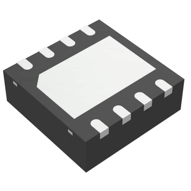
- Part No.:
- A7102CHTK2/T0BC2AJ
- Manufacturer:
- NXP Semiconductors
- Category:
- Application Specific Microcontrollers
- Package:
- 8-VDFN Exposed Pad
- Datasheet:
-
 A7102CHTK2/T0BC2AJ.pdf
- Description:
- SECURE AUTHENTICATION
- Quantity:
- Payment:

- Shipping:

Inventory:7,748
Please send an inquiry. Send us your inquiry, and we will respond immediately.
Product details
Overview
A7102CHTK2/T0BC2AJ from NXP Semiconductors is a customer-programmable security IC supporting secure authentication, key storage, and cryptographic operations (AES-128, ECDSA, SHA-256) in extended temperature range (–40 °C to +90 °C), housed in HVSON8 package, and designed for industrial IoT edge nodes requiring tamper-resistant credential management.
For engineers reviewing the A7102CHTK2/T0BC2AJ datasheet, A7102CHTK2/T0BC2AJ pinout, A7102CHTK2/T0BC2AJ application, or A7102CHTK2/T0BC2AJ equivalent, key selection criteria include operating temperature compliance, I²C interface timing, secure boot integration capability, and certified Common Criteria EAL5+ firmware execution environment.
Technical Context
The A7102CHTK2/T0BC2AJ implements a dedicated ARM SecurCore SC000-based secure processor with on-chip ROM bootloader and configurable secure memory partitions. It supports I²C communication at up to 1 MHz with clock stretching and ACK/NACK handshaking.
Its hardware-accelerated crypto engine delivers deterministic AES-128 encryption/decryption in ≤120 µs per 16-byte block and ECDSA P-256 signature generation in ≤110 ms, with all private keys isolated in non-volatile secure memory inaccessible via debug interfaces.
Key Specifications
| Parameter | Value and Actual Design Meaning |
|---|---|
| Operating Temp | –40 °C to +90 °C: Enables deployment in uncontrolled industrial enclosures and automotive under-hood environments without external thermal management. |
| Interface | I²C (1 MHz max): Supports direct connection to microcontrollers without level-shifting or protocol translation in resource-constrained edge devices. |
| Crypto Engine | AES-128, ECDSA-P256, SHA-256: Provides FIPS 140-2 Level 3 validated primitives for device identity attestation and firmware signature verification. |
| Secure Memory | 16 KB OTP + 4 KB SRAM: Stores immutable root-of-trust keys and runtime session keys with hardware-enforced read/write protection policies. |
| Security Cert | Common Criteria EAL5+: Confirmed resistance against side-channel, fault injection, and physical probing attacks per CC certification report AVA_VAN.5. |
| Package | HVSON8 (2.0 × 2.5 mm, 0.5 mm pitch): Enables high-density PCB layouts in space-constrained sensor modules and gateway SoM designs. |
Pinout & Package
HVSON8 package with wettable flank leads for automated optical inspection (AOI) and solder joint reliability in reflow-soldered industrial assemblies.
| Pin/Terminal | Circuit Role | Design Meaning |
|---|---|---|
| VDD | Power supply input | 2.7–5.5 V operation: Compatible with both 3.3 V and 5 V host system rails without external regulators. |
| GND | Ground reference | Dedicated low-impedance return path for secure logic and analog crypto circuitry to minimize noise coupling into sensitive operations. |
| SCL | I²C clock input | Open-drain, 1 MHz max: Requires external pull-up; supports clock stretching during internal crypto processing to prevent bus timeout. |
| SDA | I²C data bidirectional | Open-drain, supports ACK/NACK signaling: Ensures reliable command-response handshake for secure command sequences. |
| RST | Hardware reset input | Active-low, asynchronous: Allows full state reset of secure core independent of I²C bus activity for recovery from fault conditions. |
| NC | No connect | Internally unused pin: Must be left floating or tied to GND per layout guidelines to avoid parasitic coupling. |
| NC | No connect | Internally unused pin: Must be left floating or tied to GND per layout guidelines to avoid parasitic coupling. |
| NC | No connect | Internally unused pin: Must be left floating or tied to GND per layout guidelines to avoid parasitic coupling. |
Key Features
| Feature | Design Value |
|---|---|
| Customer programmable firmware | Enables OEM-specific secure boot flows and custom attestation protocols without NXP pre-provisioning dependency. |
| Extended temperature grade | Validated operation from –40 °C to +90 °C ensures functional integrity in outdoor gateways and factory-floor controllers. |
| Hardware crypto acceleration | Reduces host MCU CPU load by offloading AES-128 and ECDSA-P256 operations with deterministic latency. |
| Secure debug disable | Permanent JTAG/SWD disable after provisioning prevents unauthorized firmware extraction or memory dump attempts. |
| Wettable flank HVSON8 | Supports automated X-ray and AOI inspection of solder joints, improving manufacturing yield in high-reliability production lines. |
Applications
| Industrial Sensor Node | Smart Energy Meter |
|---|---|
Use Scenario: Wireless vibration sensor deployed inside HVAC compressors operating at 85 °C ambient with periodic OTA firmware updates. IC Role / Device Role / Timing Role: Secure boot root-of-trust and firmware signature verifier ensuring only signed updates execute. Use Value: Prevents malicious firmware injection during wireless update cycles while maintaining operation across thermal cycling from –40 °C startup to +90 °C steady-state. | Use Scenario: DIN-rail mounted electricity meter exposed to outdoor temperature swings and utility-grade cyberattack vectors. IC Role / Device Role / Timing Role: Hardware-backed key storage for AES-128 encryption of consumption data before transmission to AMI concentrators. Use Value: Meets IEC 62443-3-3 SL2 requirements for secure data confidentiality using certified crypto primitives and tamper-resistant memory. |
| Factory Automation PLC | Medical Diagnostic Gateway |
Use Scenario: Programmable logic controller retrofitting legacy fieldbus systems with TLS-secured cloud telemetry. IC Role / Device Role / Timing Role: ECDSA-P256 certificate signer for TLS client authentication during MQTT connections to cloud platforms. Use Value: Enables zero-touch provisioning of unique device identities without exposing private keys to PLC runtime software stack. | Use Scenario: Portable ultrasound gateway aggregating DICOM images from multiple probes and transmitting to PACS over hospital Wi-Fi. IC Role / Device Role / Timing Role: Secure key vault for HIPAA-compliant AES-256 encryption of DICOM headers and patient metadata. Use Value: Provides auditable cryptographic boundary for PHI data handling, satisfying FDA cybersecurity guidance for Class II medical devices. |
Equivalent & Alternatives
The following parts are listed as comparable options for similar security IC applications.
| Alternative Part | Technical Difference | Application Difference | Selection Advice |
|---|---|---|---|
| A7101CHTK2/T0BC2VJ | Standard temperature range (–25 °C to +85 °C); identical HVSON8 package and crypto features. | Not qualified for deployments exceeding +85 °C ambient or below –25 °C, limiting use in under-hood or outdoor infrastructure. | Select when operating environment remains within commercial temperature limits and cost sensitivity outweighs extended-range assurance. |
| A7102CHUK/T0BC2VAZ | Same extended temperature range but in WLCSP package (1.38 × 1.38 mm); no wettable flanks. | Requires advanced assembly processes (e.g., SPI solder paste, post-reflow X-ray); unsuitable for AOI-based high-volume manufacturing. | Select only for ultra-compact designs where board area savings justify process complexity and yield risk. |
Compared with A7101CHTK2/T0BC2VJ and A7102CHUK/T0BC2VAZ, the A7102CHTK2/T0BC2AJ uniquely combines extended temperature operation, HVSON8 manufacturability, and wettable flank inspection support-making it the optimal choice for industrial OEMs requiring field-deployable security without process requalification.
Availability
A7102CHTK2/T0BC2AJ is available at Aetrix Electronics and suitable for industrial IoT gateways, smart energy meters, factory automation controllers, and medical diagnostic gateways requiring stable component supply across extended temperature ranges and long product lifecycles.
Supply support for A7102CHTK2/T0BC2AJ includes scheduled delivery planning, volume procurement assistance, BOM continuity management, traceable sourcing, and lifecycle availability coordination for OEM customers, industrial embedded developers, connected-device designers, and electronics production programs.
Manufacturer
NXP Semiconductors is a global semiconductor company headquartered in Eindhoven, Netherlands, specializing in secure connectivity solutions for automotive, industrial, and IoT markets.
The A7102CHTK2/T0BC2AJ belongs to NXP's A71CH family of programmable secure elements, engineered specifically for resource-constrained edge devices needing certified cryptographic services and field-deployable tamper resistance.
FAQ
What is the maximum I²C clock frequency supported by the A7102CHTK2/T0BC2AJ?
The A7102CHTK2/T0BC2AJ supports I²C communication up to 1 MHz, with hardware-level clock stretching enabled during cryptographic operations to prevent bus timeouts. This allows seamless integration with standard I²C peripherals without requiring custom timing adjustments in the host MCU firmware. The A7102CHTK2/T0BC2AJ maintains full protocol compliance including ACK/NACK signaling and repeated START condition handling.
Does the A7102CHTK2/T0BC2AJ require external programming equipment for initial firmware loading?
No, the A7102CHTK2/T0BC2AJ supports customer programming via its standard I²C interface using NXP's A71CH SDK and host-side tools-no dedicated programmers or debug probes needed. Firmware and keys are loaded securely over I²C after power-on, with all provisioning steps authenticated and encrypted. The A7102CHTK2/T0BC2AJ does not expose JTAG or SWD interfaces post-provisioning.
How does the A7102CHTK2/T0BC2AJ differ from the A7101CHTK2/T0BC2VJ in terms of environmental qualification?
The A7102CHTK2/T0BC2AJ is qualified for –40 °C to +90 °C operation, whereas the A7101CHTK2/T0BC2VJ is rated only from –25 °C to +85 °C. This 15 °C wider lower limit and 5 °C higher upper limit enables the A7102CHTK2/T0BC2AJ to function reliably in automotive under-hood locations, outdoor utility infrastructure, and industrial enclosures without forced cooling. Both share identical electrical and cryptographic specifications.
Is the A7102CHTK2/T0BC2AJ compatible with the OM3710/A71CHARD Arduino-compatible development kit?
Yes, the A7102CHTK2/T0BC2AJ is pin-compatible and electrically compatible with the OM3710/A71CHARD Arduino-compatible development kit, which supports all A71CH family variants. The kit's firmware abstraction layer handles temperature-grade differences transparently, allowing rapid prototyping of extended-temperature secure applications using the same codebase as standard-grade variants like A7101CHTK2/T0BC2VJ.
What security certifications apply to the A7102CHTK2/T0BC2AJ firmware and hardware?
The A7102CHTK2/T0BC2AJ implements firmware and hardware validated under Common Criteria EAL5+ (certification report AVA_VAN.5), covering resistance to side-channel analysis, fault injection, and physical probing. Its cryptographic library is FIPS 140-2 Level 3 validated. These certifications apply identically across all A71CH variants, including the A7102CHTK2/T0BC2AJ, and are maintained regardless of customer programming or key provisioning.
A7102CHTK2/T0BC2AJ Specifications
- Product attributes
- Attribute value
- Manufacturer:
- NXP Semiconductors
- Series:
- A71CH
- Package/Case:
- 8-VDFN Exposed Pad
- Packaging:
- Tape & Reel (TR)
- Product Status:
- Obsolete
- Programmable:
- Not Verified
- Applications:
- Authentication
- Core Processor:
- MX51
- Program Memory Type:
- -
- Controller Series:
- -
- RAM Size:
- -
- Interface:
- I2C
- Number of I/O:
- -
- Voltage - Supply:
- 2.5V ~ 3.6V
- Operating Temperature:
- -40°C ~ 90°C (TA)
- Grade:
- -
- Qualification:
- -
- Mounting Type:
- Surface Mount
- Supplier Device Package:
- 8-HVSON (4x4)
A7102CHTK2/T0BC2AJ FAQ
1.How can I place an order for A7102CHTK2/T0BC2AJ through Aetrix?
Please submit a Request for Quotation (RFQ) for A7102CHTK2/T0BC2AJ on Aetrix. Our sales agent will provide a competitive quotation and guide you through the order confirmation once you accept the terms.
2.Are the price and stock information for A7102CHTK2/T0BC2AJ reliable?
The price and inventory of A7102CHTK2/T0BC2AJ are updated periodically and may fluctuate due to market conditions. Stock and pricing data are typically refreshed every 24 hours. Quotation validity for A7102CHTK2/T0BC2AJ is usually 5 days.
3.What payment methods are accepted for A7102CHTK2/T0BC2AJ?
We accept Wire Transfer, PayPal, Credit Card, Western Union, MoneyGram, and Escrow for A7102CHTK2/T0BC2AJ transactions.
Note: Certain payment methods may incur a processing fee.
4.How is shipping managed for A7102CHTK2/T0BC2AJ?
A7102CHTK2/T0BC2AJ orders can be shipped via leading logistics carriers, including DHL, UPS, FedEx, TNT, or Registered Mail.
Once your A7102CHTK2/T0BC2AJ order is processed, you will receive an email with the shipment details and tracking number.
Note: Tracking information may take up to 24 hours to appear. Express delivery typically takes 3–5 business days.
5.How can I obtain technical support or documentation for A7102CHTK2/T0BC2AJ?
For technical support, including A7102CHTK2/T0BC2AJ datasheets, pinout diagrams, or application guidance, please contact our engineering support team. They can provide detailed documentation and assistance for your A7102CHTK2/T0BC2AJ requirements.
6.How does Aetrix verify that A7102CHTK2/T0BC2AJ is sourced from the original manufacturer or authorized distributors?
All A7102CHTK2/T0BC2AJ products on Aetrix are procured from qualified distributors and authorized channels. Our dedicated quality assurance team conducts strict verification, including traceability checks and, if necessary, third-party testing. This ensures that A7102CHTK2/T0BC2AJ meets industry standards.
7.What is the process for return or replacement of A7102CHTK2/T0BC2AJ?
All A7102CHTK2/T0BC2AJ units undergo pre-shipment inspection (PSI). If there is an issue with A7102CHTK2/T0BC2AJ, returns or replacements are accepted under the following conditions:
1.Quantity discrepancies, incorrect items, or visible external defects (such as breakage or corrosion), acknowledged by Aetrix.
2.The issue is reported within 90 days of delivery.
3.The A7102CHTK2/T0BC2AJ part is unused and in its original packaging.
Return procedure for A7102CHTK2/T0BC2AJ:
1.Submit a request within 90 days.
2.Obtain a Return Material Authorization (RMA) from Aetrix.
A7102CHTK2/T0BC2AJ Tags

-
CYPD3175-24LQXQ
Infineon Technologies

-
SLB9672VU20FW1523XTMA1
Infineon Technologies

-
SLB9670VQ20FW785XTMA1
Infineon Technologies
-
SLB9672XU20FW1523XTMA1
Infineon Technologies
-
SLB9673XU20FW2613XTMA1
Infineon Technologies

-
CYPD3125-40LQXIT
Infineon Technologies

-
AT97SC3204-U2A1A-20
Microchip Technology
-
AT97SC3204-U2A1A-10
Microchip Technology
-
SLM9670AQ20FW1311XTMA1
Infineon Technologies
-
SLB9672XU20FW1613XTMA1
Infineon Technologies
-
SLB9672AU20FW1613XTMA1
Infineon Technologies
-
SLB9673AU20FW2613XTMA1
Infineon Technologies
Tech Hub

A practical engineering guide to 3.3V and 5V logic compatibility, input thresholds, resistor dividers, translator ICs, MOSFET level shifting, I2C pull-ups, timing limits and power-sequencing risks.

The 74HC595 uses push-pull logic outputs, while the TPIC6B595 uses 50 V open-drain DMOS sinks for higher-power loads. This guide compares timing, current limits, 3.3 V interfacing, load wiring, thermal…

The 74HC595 converts serial data into eight stable parallel outputs. This guide covers pin functions, shift and storage timing, OE and MR behavior, drive-current limits, cascading, voltage compatibilit…

A technical comparison of level-sensitive latches and edge-triggered flip-flops, covering timing windows, setup and hold limits, master–slave operation, time borrowing, race-through, HDL inference and…

A D latch stores one bit while Enable controls when data can pass. This reference covers gate-level operation, truth tables, transparency, setup and hold timing, LE versus OE, common ICs and practical …

An SR latch stores one bit through cross-coupled feedback. This engineering reference covers NOR and NAND implementations, truth tables, forbidden-state recovery, gated operation, switch debouncing, fa…

Latch circuits retain one bit through feedback. This technical reference covers SR and D latches, truth tables, transparency, timing limits, latch-versus-flip-flop behavior, applications and common log…

An engineering guide to LED driver operation, constant-current and constant-voltage outputs, linear and switching topologies, dimming, IC selection, calculations, replacement compatibility, and fault c…

Operational amplifier guide covering op amp basics, feedback, ideal vs real op amps, common configurations, buffer circuits, offset, bias current, gain-bandwidth, slew rate, rail-to-rail limits and sel…

Jumper cables guide covering safe connection order, red and black clamp placement, final ground connection, cable gauge, length, clamp quality, copper vs CCA cables, jump starter comparison and battery…


