
 My Inquiry
 My Account


NXP Semiconductors A7102CHTK2/T0BC2CJ
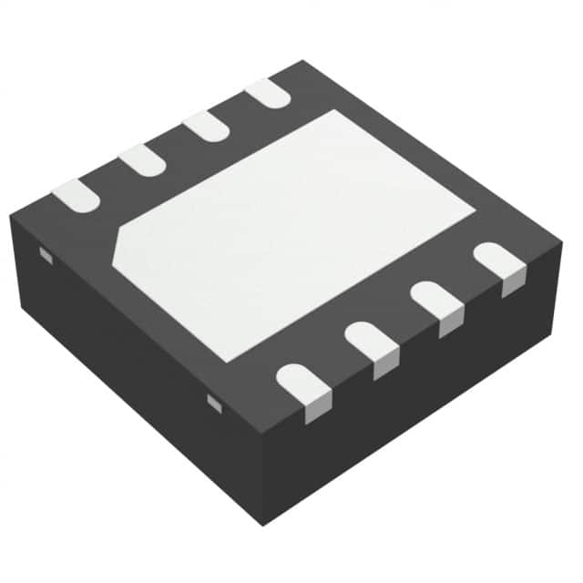
- Part No.:
- A7102CHTK2/T0BC2CJ
- Manufacturer:
- NXP Semiconductors
- Category:
- Application Specific Microcontrollers
- Package:
- 8-VDFN Exposed Pad
- Datasheet:
-
 A7102CHTK2/T0BC2CJ.pdf
- Description:
- SECURITY IC EXT TEMP HVSON8
- Quantity:
- Payment:

- Shipping:

Inventory:4,822
Please send an inquiry. Send us your inquiry, and we will respond immediately.
Product details
Overview
A7102CHTK2/T0BC2CJ from NXP Semiconductors is a customer-provisioned security IC with extended temperature range (−40 °C to +90 °C), supporting IBM Watson IoT platform integration, featuring secure boot, cryptographic acceleration (AES-128, SHA-256, ECDSA), and tamper-resistant key storage in HVSON8 package.
For engineers reviewing the A7102CHTK2/T0BC2CJ datasheet, A7102CHTK2/T0BC2CJ pinout, A7102CHTK2/T0BC2CJ application, or A7102CHTK2/T0BC2CJ equivalent, this device serves as a pre-provisioned, IoT-edge-ready secure element for cloud-connected industrial sensors, gateway authentication, and firmware integrity verification under harsh thermal conditions.
Technical Context
The A7102CHTK2/T0BC2CJ implements a dedicated secure execution environment with ARM TrustZone-assisted isolation, hardened against side-channel and fault injection attacks. It supports TLS 1.2/1.3 handshake offload and X.509 certificate chain validation using on-chip ECC P-256 key generation and storage.
It interfaces exclusively via I²C (up to 1 MHz) with configurable slave address and hardware reset input, requiring no external voltage regulators - operating from 1.71 V to 3.6 V with internal LDO regulation and brown-out detection at 1.62 V.
Key Specifications
| Parameter | Value and Actual Design Meaning |
|---|---|
| Operating Temp | −40 °C to +90 °C: Enables deployment in uncontrolled industrial enclosures and outdoor edge nodes without thermal derating. |
| Crypto Engine | AES-128, SHA-256, ECDSA P-256: Hardware-accelerated signing/verification for firmware updates and device attestation. |
| Interface | I²C up to 1 MHz: Compatible with standard microcontroller I/O without custom timing or level-shifting circuitry. |
| Supply Voltage | 1.71 V–3.6 V with internal LDO: Simplifies power design by eliminating need for external low-noise regulators. |
| Package | HVSON8 (2.0 × 2.5 mm, 0.5 mm pitch): Supports high-density PCB layouts and automated optical inspection. |
| Provisioning State | Pre-provisioned for IBM Watson IoT: Contains factory-programmed credentials and root-of-trust keys for immediate cloud onboarding. |
Pinout & Package
HVSON8 package: 2.0 mm × 2.5 mm body, 0.5 mm lead pitch, exposed thermal pad, JEDEC MO-220 compliant.
| Pin/Terminal | Circuit Role | Design Meaning |
|---|---|---|
| VDD | Power supply input | Accepts 1.71–3.6 V; internal LDO regulates core logic and crypto engine. |
| GND | Ground reference | Common return path for digital and analog domains; connects to exposed thermal pad. |
| SCL | I²C clock input | Active-high, supports standard/fast-mode I²C up to 1 MHz; internal pull-up not provided. |
| SDA | I²C data bidirectional | Open-drain, requires external pull-up; handles command/response framing per NXP A710x protocol stack. |
| RST | Hardware reset input | Active-low asynchronous reset; debounced internally; asserts secure state on deassertion. |
| INT | Interrupt output | Open-drain status signal indicating completion of crypto operation or error condition. |
| NC | No connect | Pin 7 is unconnected; must be left floating or tied to GND per layout guidelines. |
| EPAD | Thermal & electrical ground | Exposed pad beneath package; soldered to PCB ground plane for thermal dissipation and noise reduction. |
Key Features
| Feature | Design Value |
|---|---|
| IBM Watson IoT Ready | Factory-provisioned with Watson-compatible credentials, TLS root CA, and device identity certificate - enables zero-touch onboarding. |
| Tamper-Resistant Key Storage | Dedicated non-volatile memory with physical protection against probing, glitching, and decapsulation; keys never exposed outside secure boundary. |
| Secure Boot Support | Verifies signed firmware images prior to execution using embedded public key; prevents unauthorized or corrupted code execution. |
| Side-Channel Resilience | Masked AES and constant-time ECC implementations mitigate timing and power analysis attacks during cryptographic operations. |
| Extended Temperature Operation | Validated functionality across −40 °C to +90 °C ensures reliability in industrial gateways, smart meters, and automotive telematics edge nodes. |
Applications
| Industrial Sensor Node Security | Smart Meter Authentication |
|---|---|
Use Scenario: Wireless temperature/humidity sensor deployed in factory floor environments with ambient temperatures up to 85 °C and transient spikes to 90 °C. IC Role / Device Role / Timing Role: Secure element performing mutual TLS authentication and encrypted payload signing before transmission to edge gateway. Use Value: Prevents spoofed sensor data injection by enforcing cryptographic identity binding and firmware integrity checks at boot and runtime. | Use Scenario: Electricity meter with remote firmware update capability and regulatory compliance for EU Measuring Instruments Directive (MID). IC Role / Device Role / Timing Role: Root-of-trust anchor storing private keys for digital signature of consumption logs and update packages. Use Value: Ensures auditability and non-repudiation of energy data while meeting EN 13757-3 and IEC 62056-47 security requirements. |
| IIoT Gateway Identity | Connected Building Controller |
Use Scenario: Edge gateway aggregating Modbus RTU devices and forwarding to IBM Watson IoT Cloud via MQTT over TLS. IC Role / Device Role / Timing Role: Hardware-backed TLS 1.2/1.3 session establishment and certificate chain validation for secure cloud channel setup. Use Value: Offloads CPU-intensive crypto operations from host MCU and eliminates software-based key exposure risk during handshake. | Use Scenario: HVAC controller installed in rooftop units exposed to direct sunlight and wide diurnal temperature swings. IC Role / Device Role / Timing Role: Secure boot verifier and runtime attestation agent ensuring only authorized firmware executes after power cycle. Use Value: Mitigates ransomware-style firmware corruption and enforces OEM-controlled update policy in safety-critical building systems. |
Equivalent & Alternatives
The following parts are listed as comparable options for similar secure element applications.
| Alternative Part | Technical Difference | Application Difference | Selection Advice |
|---|---|---|---|
| A7102CHTK2/T0BC2AJ | Same silicon, same HVSON8 package, but factory-provisioned for generic use - lacks IBM Watson IoT credentials and preloaded root CA. | Requires customer-side credential provisioning and TLS stack integration; suitable for private cloud or on-premise deployments. | Select when full control over identity lifecycle is required and Watson IoT integration is not mandated. |
| SE050M1014 | NXP SE050 family; supports additional protocols (SCP03, ISO 7816-4), higher ECC key sizes (P-384), and optional contactless interface. | Broadens support to payment-grade and government ID applications; increases BOM cost and firmware complexity. | Select when multi-protocol compliance (e.g., FIDO2, eIDAS) or future-proofing beyond Watson IoT is needed. |
Compared with A7102CHTK2/T0BC2AJ and SE050M1014, the A7102CHTK2/T0BC2CJ delivers shortest time-to-cloud for IBM Watson IoT deployments due to factory-provisioned credentials, while maintaining identical thermal robustness and cryptographic capabilities - ideal for rapid industrial IoT prototyping and volume rollout.
Availability
A7102CHTK2/T0BC2CJ is available at Aetrix Electronics and suitable for industrial sensor nodes, smart metering systems, IIoT gateways, and connected building controllers requiring stable component supply across extended temperature ranges.
Supply support for A7102CHTK2/T0BC2CJ includes scheduled delivery planning, volume procurement assistance, BOM continuity management, traceable sourcing, and lifecycle availability coordination for OEM customers, industrial embedded developers, connected-device designers, and electronics production programs.
Manufacturer
NXP Semiconductors is a global semiconductor company headquartered in Eindhoven, Netherlands, specializing in secure connectivity solutions for automotive, industrial, and IoT markets.
The A710x series is designed specifically for resource-constrained edge devices needing certified, pre-provisioned security - targeting rapid cloud onboarding, firmware integrity, and regulatory-compliant identity management.
FAQ
Is A7102CHTK2/T0BC2CJ pin-compatible with A7101CHTK2/T0BC2BJ?
Yes, A7102CHTK2/T0BC2CJ is pin-compatible with A7101CHTK2/T0BC2BJ - both use identical HVSON8 package, I²C interface mapping, and power pinout. The difference lies in temperature rating (−40 °C to +90 °C vs. −25 °C to +85 °C) and provisioning content (IBM Watson IoT vs. generic). No PCB redesign is needed for migration.
Does A7102CHTK2/T0BC2CJ require external firmware programming after purchase?
No, A7102CHTK2/T0BC2CJ ships pre-provisioned with IBM Watson IoT credentials, including device identity certificate, root CA bundle, and private key securely stored in tamper-resistant memory. Customers can initiate cloud onboarding immediately without any provisioning step - A7102CHTK2/T0BC2CJ is ready for TLS handshake out of the box.
What cryptographic algorithms does A7102CHTK2/T0BC2CJ accelerate in hardware?
A7102CHTK2/T0BC2CJ accelerates AES-128 (ECB/CBC/GCM modes), SHA-256, and ECDSA with NIST P-256 curve in dedicated hardware. These engines support secure boot signature verification, firmware update signing, and TLS 1.2/1.3 handshake offload - all without exposing keys to host software or external memory.
Can A7102CHTK2/T0BC2CJ operate reliably at 90 °C ambient temperature?
Yes, A7102CHTK2/T0BC2CJ is fully characterized and guaranteed to operate across −40 °C to +90 °C ambient temperature. Its thermal design, including the exposed pad and internal LDO, maintains junction temperature within safe limits even under sustained 90 °C ambient with typical I²C traffic - validated per JEDEC JESD22-A104 thermally accelerated stress testing.
How does A7102CHTK2/T0BC2CJ handle secure boot verification?
A7102CHTK2/T0BC2CJ performs secure boot by verifying the digital signature of the host MCU's firmware image using its embedded P-256 public key. The signature is checked before execution begins; if invalid or missing, the device halts boot and asserts RST. This process is enforced in hardware and cannot be bypassed - A7102CHTK2/T0BC2CJ ensures only cryptographically authenticated code runs on the system.
A7102CHTK2/T0BC2CJ Specifications
- Product attributes
- Attribute value
- Manufacturer:
- NXP Semiconductors
- Series:
- A71CH
- Package/Case:
- 8-VDFN Exposed Pad
- Packaging:
- Tape & Reel (TR)
- Product Status:
- Obsolete
- Programmable:
- Not Verified
- Applications:
- Authentication
- Core Processor:
- MX51
- Program Memory Type:
- -
- Controller Series:
- -
- RAM Size:
- -
- Interface:
- I2C
- Number of I/O:
- -
- Voltage - Supply:
- 2.5V ~ 3.6V
- Operating Temperature:
- -40°C ~ 90°C (TA)
- Grade:
- -
- Qualification:
- -
- Mounting Type:
- Surface Mount
- Supplier Device Package:
- 8-HVSON (4x4)
A7102CHTK2/T0BC2CJ FAQ
1.How can I place an order for A7102CHTK2/T0BC2CJ through Aetrix?
Please submit a Request for Quotation (RFQ) for A7102CHTK2/T0BC2CJ on Aetrix. Our sales agent will provide a competitive quotation and guide you through the order confirmation once you accept the terms.
2.Are the price and stock information for A7102CHTK2/T0BC2CJ reliable?
The price and inventory of A7102CHTK2/T0BC2CJ are updated periodically and may fluctuate due to market conditions. Stock and pricing data are typically refreshed every 24 hours. Quotation validity for A7102CHTK2/T0BC2CJ is usually 5 days.
3.What payment methods are accepted for A7102CHTK2/T0BC2CJ?
We accept Wire Transfer, PayPal, Credit Card, Western Union, MoneyGram, and Escrow for A7102CHTK2/T0BC2CJ transactions.
Note: Certain payment methods may incur a processing fee.
4.How is shipping managed for A7102CHTK2/T0BC2CJ?
A7102CHTK2/T0BC2CJ orders can be shipped via leading logistics carriers, including DHL, UPS, FedEx, TNT, or Registered Mail.
Once your A7102CHTK2/T0BC2CJ order is processed, you will receive an email with the shipment details and tracking number.
Note: Tracking information may take up to 24 hours to appear. Express delivery typically takes 3–5 business days.
5.How can I obtain technical support or documentation for A7102CHTK2/T0BC2CJ?
For technical support, including A7102CHTK2/T0BC2CJ datasheets, pinout diagrams, or application guidance, please contact our engineering support team. They can provide detailed documentation and assistance for your A7102CHTK2/T0BC2CJ requirements.
6.How does Aetrix verify that A7102CHTK2/T0BC2CJ is sourced from the original manufacturer or authorized distributors?
All A7102CHTK2/T0BC2CJ products on Aetrix are procured from qualified distributors and authorized channels. Our dedicated quality assurance team conducts strict verification, including traceability checks and, if necessary, third-party testing. This ensures that A7102CHTK2/T0BC2CJ meets industry standards.
7.What is the process for return or replacement of A7102CHTK2/T0BC2CJ?
All A7102CHTK2/T0BC2CJ units undergo pre-shipment inspection (PSI). If there is an issue with A7102CHTK2/T0BC2CJ, returns or replacements are accepted under the following conditions:
1.Quantity discrepancies, incorrect items, or visible external defects (such as breakage or corrosion), acknowledged by Aetrix.
2.The issue is reported within 90 days of delivery.
3.The A7102CHTK2/T0BC2CJ part is unused and in its original packaging.
Return procedure for A7102CHTK2/T0BC2CJ:
1.Submit a request within 90 days.
2.Obtain a Return Material Authorization (RMA) from Aetrix.
A7102CHTK2/T0BC2CJ Tags

-
CYPD3175-24LQXQ
Infineon Technologies

-
SLB9672VU20FW1523XTMA1
Infineon Technologies

-
SLB9670VQ20FW785XTMA1
Infineon Technologies
-
SLB9672XU20FW1523XTMA1
Infineon Technologies
-
SLB9673XU20FW2613XTMA1
Infineon Technologies

-
CYPD3125-40LQXIT
Infineon Technologies

-
AT97SC3204-U2A1A-20
Microchip Technology
-
AT97SC3204-U2A1A-10
Microchip Technology
-
SLM9670AQ20FW1311XTMA1
Infineon Technologies
-
SLB9672XU20FW1613XTMA1
Infineon Technologies
-
SLB9672AU20FW1613XTMA1
Infineon Technologies
-
SLB9673AU20FW2613XTMA1
Infineon Technologies
Tech Hub

A practical engineering guide to 3.3V and 5V logic compatibility, input thresholds, resistor dividers, translator ICs, MOSFET level shifting, I2C pull-ups, timing limits and power-sequencing risks.

The 74HC595 uses push-pull logic outputs, while the TPIC6B595 uses 50 V open-drain DMOS sinks for higher-power loads. This guide compares timing, current limits, 3.3 V interfacing, load wiring, thermal…

The 74HC595 converts serial data into eight stable parallel outputs. This guide covers pin functions, shift and storage timing, OE and MR behavior, drive-current limits, cascading, voltage compatibilit…

A technical comparison of level-sensitive latches and edge-triggered flip-flops, covering timing windows, setup and hold limits, master–slave operation, time borrowing, race-through, HDL inference and…

A D latch stores one bit while Enable controls when data can pass. This reference covers gate-level operation, truth tables, transparency, setup and hold timing, LE versus OE, common ICs and practical …

An SR latch stores one bit through cross-coupled feedback. This engineering reference covers NOR and NAND implementations, truth tables, forbidden-state recovery, gated operation, switch debouncing, fa…

Latch circuits retain one bit through feedback. This technical reference covers SR and D latches, truth tables, transparency, timing limits, latch-versus-flip-flop behavior, applications and common log…

An engineering guide to LED driver operation, constant-current and constant-voltage outputs, linear and switching topologies, dimming, IC selection, calculations, replacement compatibility, and fault c…

Operational amplifier guide covering op amp basics, feedback, ideal vs real op amps, common configurations, buffer circuits, offset, bias current, gain-bandwidth, slew rate, rail-to-rail limits and sel…

Jumper cables guide covering safe connection order, red and black clamp placement, final ground connection, cable gauge, length, clamp quality, copper vs CCA cables, jump starter comparison and battery…


