
 My Inquiry
 My Account


Analog Devices Inc. ADN8834ACPZ-R7
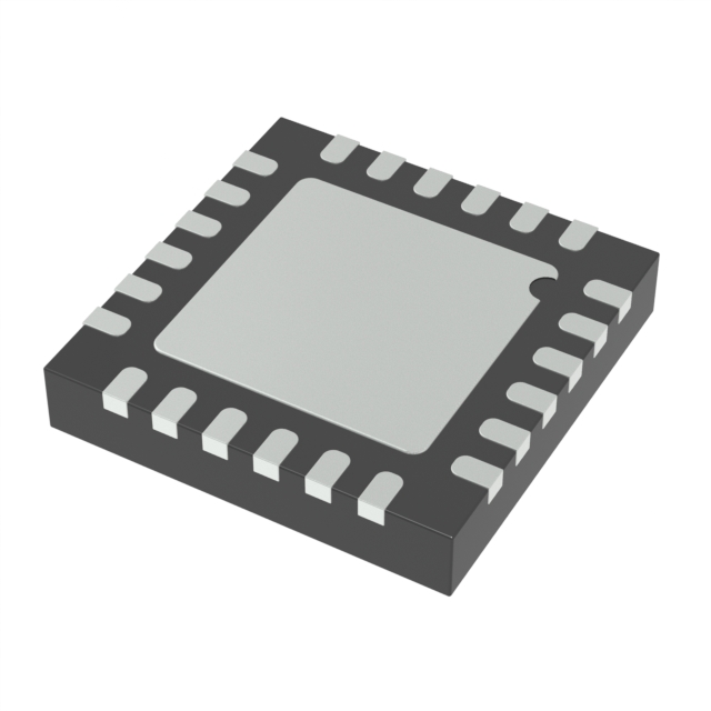
- Part No.:
- ADN8834ACPZ-R7
- Manufacturer:
- Analog Devices Inc.
- Category:
- Power Management - Specialized
- Package:
- 24-WFQFN Exposed Pad, CSP
- Datasheet:
-
 ADN8834ACPZ-R7.pdf
- Description:
- IC THERMO COOLER DRIVER 24LFCSP
- Quantity:
- Payment:

- Shipping:

Inventory:157
Please send an inquiry. Send us your inquiry, and we will respond immediately.
Product details
Overview
ADN8834ACPZ-R7 from Analog Devices is an ultracompact, monolithic thermoelectric cooler (TEC) controller with integrated 1.5 A H-bridge power stage, dual zero-drift chopper amplifiers, 2.0 MHz PWM switching, programmable heating/cooling current limits, and 2.50 V ±1% reference output. It enables precise analog PID temperature stabilization for laser diodes in optical transceivers.
For engineers reviewing the ADN8834ACPZ-R7 datasheet, ADN8834ACPZ-R7 pinout, ADN8834ACPZ-R7 application, or ADN8834ACPZ-R7 equivalent, key selection considerations include TEC voltage/current monitoring accuracy (±10% at 700–1500 mA), independent cooling/heating current limit configuration via ILIM pin, bidirectional voltage limiting via VLIM/SD, thermal lock indication (LFCSP only), and AEC-Q100 qualification for automotive optical modules.
Technical Context
The ADN8834ACPZ-R7 implements a hybrid linear-PWM H-bridge architecture: one side uses a linear driver (LDR) with 1.5 A max source/sink capability and low RDS(ON) (31–50 mΩ N-MOSFET, WLCSP), while the other uses a 2.0 MHz PWM driver (SW/SFB) with synchronous rectification. This patented single-inductor topology achieves >90% efficiency without external sense resistors.
Its two rail-to-rail chopper amplifiers support autonomous analog PID control-Chopper 1 conditions NTC/RTD sensor signals into proportional temperature voltage (OUT1), and Chopper 2 serves as error amplifier/compensator (IN2P/IN2N/OUT2) with 2 MHz GBW and <100 µV offset. The internal 2.50 V reference biases both sensor bridges and limit-setting networks.
Key Specifications
| Parameter | Value and Actual Design Meaning |
|---|---|
| Max TEC Current | ±1.5 A (TJ ≤ +105°C); enables direct drive of medium-power TECs without external FETs |
| PWM Frequency | 2.0 MHz typical; allows use of compact 1 µH inductor and 10 µF capacitor for low-ripple output |
| Reference Voltage | 2.50 V ±1%; provides stable bias for thermistor bridges and precision limit programming |
| Current Sense Accuracy | ±10% (700–1500 mA, WLCSP); eliminates need for external shunt while maintaining closed-loop stability |
| Voltage Sense Gain | 0.25 V/V; maps ±4 V TEC differential voltage to 0.005–2.625 V VTEC output for ADC interfacing |
| Supply Range | 2.7 V to 5.5 V on VDD and PVIN; supports single-supply operation from common 3.3 V or 5 V rails |
| Thermal Shutdown | 170°C threshold with 17°C hysteresis; protects device during sustained overload or poor heatsinking |
Pinout & Package
ADN8834ACPZ-R7 is packaged in a 25-ball, 2.5 mm × 2.5 mm WLCSP (Wafer-Level Chip Scale Package) with exposed EPAD for thermal management. Pin assignments are ball-grid mapped per JEDEC MO-255; no leadframe or gull-wing leads.
| Pin/Terminal | Circuit Role | Design Meaning |
|---|---|---|
| LDR | Linear Driver Output | H-bridge low-side linear output; delivers ±1.5 A with <50 mΩ RDS(ON) (WLCSP) |
| SW | PWM Switch Node | H-bridge high-side PWM output; switches at 2.0 MHz with synchronous rectification |
| ITEC | TEC Current Monitor | Analog output: 1.25 V ± ILDR × 0.525 V/A; enables real-time current feedback without shunt |
| VTEC | TEC Voltage Monitor | Analog output: 1.25 V + 0.25 × (VLDR − VSFB); measures ±4 V differential across TEC |
| ILIM | Current Limit Control | Analog input setting independent cooling (1.3–2.3 V) and heating (0.2–1.2 V) current thresholds |
| VLIM/SD | Voltage Limit / Shutdown | Bidirectional voltage limiter input; pull ≤0.07 V to force shutdown; sets asymmetric cooling/heating voltage caps |
| EN/SY | Enable / Sync Input | Logic-enable (≥2.1 V) or external sync clock input (1.85–3.25 MHz); no external oscillator needed |
| VREF | 2.50 V Reference | 1% accurate, 10 mA capable output; used for sensor biasing and limit network calibration |
| PGNDL / PGNDS | Power Grounds | Separate grounds for linear (PGNDL) and PWM (PGNDS) sections minimize noise coupling |
| AGND | Signal Ground | Analog ground reference for amplifiers, references, and monitor outputs; must be star-connected |
Key Features
| Feature | Design Value |
|---|---|
| Patented single-inductor H-bridge | Eliminates second inductor and reduces BOM count by 30% vs. dual-PWM architectures |
| Integrated MOSFETs with low RDS(ON) | 31–50 mΩ (N-MOSFET, WLCSP) enables >90% efficiency at 1 A with minimal thermal derating |
| Dual zero-drift chopper amplifiers | 10 µV offset, 2 MHz GBW, 120 dB CMRR - sustains <0.01°C long-term thermal stability |
| No external sense resistor required | On-chip current sensing reduces layout area, cost, and thermal drift errors in precision loops |
| Independent heating/cooling current limits | Enables asymmetric thermal response tuning - e.g., faster cooling than heating for laser transient suppression |
Applications
| Optical Transceivers | Laser Diode Modules |
|---|---|
Use Scenario: Stabilizing temperature of DFB/FP laser diodes in 100G–400G QSFP-DD and OSFP pluggable modules operating from −5°C to +70°C ambient. IC Role / Device Role / Timing Role: Primary TEC controller executing analog PID loop; drives TEC directly using LDR/SW outputs while monitoring ITEC/VTEC for closed-loop correction. Use Value: Maintains laser wavelength within ±0.1 nm via sub-0.02°C thermal stability, meeting ITU-T G.698.2 spectral compliance without FPGA-based digital compensation. | Use Scenario: Temperature regulation of pump lasers in erbium-doped fiber amplifiers (EDFAs) deployed in metro/core DWDM networks. IC Role / Device Role / Timing Role: Monolithic TEC driver with integrated reference and amplifiers; interfaces directly to NTC thermistor and DAC-setpoint circuitry for autonomous analog control. Use Value: Achieves <15 ms thermal settling time after ambient step change, enabling fast channel provisioning and reducing EDFA gain transient-induced BER spikes. |
| Fiber Optic Test Equipment | Automotive LiDAR Emitters |
Use Scenario: Precision temperature control of tunable lasers in optical spectrum analyzers and wavelength meters requiring <0.005 nm resolution. IC Role / Device Role / Timing Role: High-accuracy analog TEC controller with ±10% current sensing and 0.25 V/V voltage scaling for calibrated feedback to external 16-bit ADC. Use Value: Enables traceable calibration against NIST standards by eliminating gain drift in external sense paths and reference buffers. | Use Scenario: Thermal stabilization of 905 nm VCSEL arrays in automotive-grade solid-state LiDAR systems operating across −40°C to +105°C junction range. IC Role / Device Role / Timing Role: AEC-Q100 qualified TEC controller managing bidirectional heat pumping under pulsed 10 A peak load conditions. Use Value: Prevents VCSEL wavelength shift beyond 905 ± 3 nm tolerance during rapid ambient transitions, ensuring consistent time-of-flight measurement accuracy. |
Equivalent & Alternatives
The following parts are listed as comparable options for similar TEC controller applications.
| Alternative Part | Technical Difference | Application Difference | Selection Advice |
|---|---|---|---|
| ADN8833ACPZ-R7 | Same 24-lead LFCSP package option; digital-only PID control path; no analog OUT1/OUT2 chopper amplifier outputs | Lacks autonomous analog loop capability; requires external MCU for full PID implementation | Select when system already includes high-performance microcontroller and firmware-defined thermal algorithms are preferred |
| MAX1968EUB+ | Higher 3 A output; 3.5 MHz switching; no integrated reference or chopper amplifiers; requires external op-amps and 2.5 V reference | Needs ≥6 additional passives for sensor interface and compensation; larger PCB footprint | Select when driving high-power TECs (>2 A) and board space permits discrete signal conditioning components |
Compared with ADN8834ACPZ-R7, ADN8833ACPZ-R7 removes analog PID autonomy but reduces cost for digitally controlled systems, while MAX1968EUB+ trades integration for higher current and frequency - requiring added design effort for sensor biasing, amplification, and reference stability.
Availability
ADN8834ACPZ-R7 is available at Aetrix Electronics and suitable for optical transceivers, laser diode modules, fiber test equipment, and automotive LiDAR systems requiring stable component supply, AEC-Q100 compliance, and long-lifecycle support.
Supply support for ADN8834ACPZ-R7 includes scheduled delivery planning, volume procurement assistance, BOM continuity management, traceable sourcing, and lifecycle availability coordination for OEM customers, industrial embedded developers, connected-device designers, and electronics production programs.
Manufacturer
Analog Devices, Inc. is a global semiconductor leader specializing in high-performance analog, mixed-signal, and digital signal processing technologies for precision instrumentation, communications, and industrial applications.
The ADN8834ACPZ-R7 belongs to Analog Devices' TEC controller product line, designed specifically for compact, high-efficiency thermal stabilization of laser diodes and photonic components in space-constrained optical modules.
FAQ
What is the maximum continuous TEC current supported by the ADN8834ACPZ-R7?
The ADN8834ACPZ-R7 supports ±1.5 A continuous TEC current at junction temperatures up to +105°C. At +125°C, the maximum rating reduces to ±1.2 A due to thermal derating. These values apply to the WLCSP package (ADN8834ACPZ-R7) and are validated across the full 2.7 V to 5.5 V supply range. The device implements hiccup-mode protection if LDR current exceeds 2.2 A.
Does the ADN8834ACPZ-R7 require an external sense resistor for current monitoring?
No, the ADN8834ACPZ-R7 does not require an external sense resistor. It integrates on-die current sensing with a fixed gain of 0.525 V/A, delivering a ratiometric voltage on the ITEC pin (1.25 V ± ILDR × 0.525 V/A). This architecture eliminates shunt-related errors, power loss, and PCB area while maintaining ±10% accuracy over 700–1500 mA in the WLCSP variant.
How does the ADN8834ACPZ-R7 implement independent heating and cooling current limits?
The ADN8834ACPZ-R7 uses the ILIM pin to set separate thresholds: cooling current limit is triggered when ILIM voltage is 1.3–2.3 V (typ. 2.0 V), while heating limit activates at 0.2–1.2 V (typ. 0.5 V). Internal current sources/sinks detect polarity and scale the limit accordingly. This allows asymmetric thermal response - for example, 1.2 A cooling / 0.8 A heating - critical for minimizing laser wavelength overshoot during mode transitions.
Can the ADN8834ACPZ-R7 operate with a 3.3 V supply only, or does it require separate 5 V rails?
The ADN8834ACPZ-R7 operates fully from a single 3.3 V supply applied to both VDD and PVIN pins. Its 2.7 V to 5.5 V input range ensures compatibility with standard logic rails. No separate 5 V rail is needed - all internal circuits, including the 2.50 V reference and MOSFET drivers, function correctly at 3.3 V, with verified performance down to 2.7 V under worst-case load and temperature conditions.
Is the ADN8834ACPZ-R7 pin-compatible with other devices in the ADN883x family?
No, the ADN8834ACPZ-R7 (25-ball WLCSP) is not pin-compatible with ADN8833ACPZ-R7 (24-lead LFCSP) or ADN8831. While functional blocks overlap, pin counts, ball/lead mappings, and power domain assignments differ significantly - e.g., ADN8834ACPZ-R7 merges PGNDL/PGNDS into shared balls, whereas ADN8833 separates them. Board redesign is required for substitution; refer to respective pin configuration diagrams in Rev. C datasheet.
ADN8834ACPZ-R7 Specifications
- Product attributes
- Attribute value
- Manufacturer:
- Analog Devices Inc.
- Series:
- -
- Package/Case:
- 24-WFQFN Exposed Pad, CSP
- Packaging:
- Tape & Reel (TR)
- Product Status:
- Active
- Applications:
- Thermoelectric Cooler
- Current - Supply:
- 3.3mA
- Voltage - Supply:
- 2.7V ~ 5.5V
- Operating Temperature:
- -40°C ~ 125°C
- Grade:
- -
- Qualification:
- -
- Mounting Type:
- Surface Mount
- Supplier Device Package:
- 24-LFCSP (4x4)
ADN8834ACPZ-R7 FAQ
1.How can I place an order for ADN8834ACPZ-R7 through Aetrix?
Please submit a Request for Quotation (RFQ) for ADN8834ACPZ-R7 on Aetrix. Our sales agent will provide a competitive quotation and guide you through the order confirmation once you accept the terms.
2.Are the price and stock information for ADN8834ACPZ-R7 reliable?
The price and inventory of ADN8834ACPZ-R7 are updated periodically and may fluctuate due to market conditions. Stock and pricing data are typically refreshed every 24 hours. Quotation validity for ADN8834ACPZ-R7 is usually 5 days.
3.What payment methods are accepted for ADN8834ACPZ-R7?
We accept Wire Transfer, PayPal, Credit Card, Western Union, MoneyGram, and Escrow for ADN8834ACPZ-R7 transactions.
Note: Certain payment methods may incur a processing fee.
4.How is shipping managed for ADN8834ACPZ-R7?
ADN8834ACPZ-R7 orders can be shipped via leading logistics carriers, including DHL, UPS, FedEx, TNT, or Registered Mail.
Once your ADN8834ACPZ-R7 order is processed, you will receive an email with the shipment details and tracking number.
Note: Tracking information may take up to 24 hours to appear. Express delivery typically takes 3–5 business days.
5.How can I obtain technical support or documentation for ADN8834ACPZ-R7?
For technical support, including ADN8834ACPZ-R7 datasheets, pinout diagrams, or application guidance, please contact our engineering support team. They can provide detailed documentation and assistance for your ADN8834ACPZ-R7 requirements.
6.How does Aetrix verify that ADN8834ACPZ-R7 is sourced from the original manufacturer or authorized distributors?
All ADN8834ACPZ-R7 products on Aetrix are procured from qualified distributors and authorized channels. Our dedicated quality assurance team conducts strict verification, including traceability checks and, if necessary, third-party testing. This ensures that ADN8834ACPZ-R7 meets industry standards.
7.What is the process for return or replacement of ADN8834ACPZ-R7?
All ADN8834ACPZ-R7 units undergo pre-shipment inspection (PSI). If there is an issue with ADN8834ACPZ-R7, returns or replacements are accepted under the following conditions:
1.Quantity discrepancies, incorrect items, or visible external defects (such as breakage or corrosion), acknowledged by Aetrix.
2.The issue is reported within 90 days of delivery.
3.The ADN8834ACPZ-R7 part is unused and in its original packaging.
Return procedure for ADN8834ACPZ-R7:
1.Submit a request within 90 days.
2.Obtain a Return Material Authorization (RMA) from Aetrix.
ADN8834ACPZ-R7 Tags

-
TPS2511DGNR
Texas Instruments

-
UTC2000/MG
Microchip Technology

-
TUSB320HAIRWBR
Texas Instruments

-
TPS61252DSGR
Texas Instruments

-
PI5USB30216CXUAEX
Diodes Incorporated

-
SN6501DBVR
Texas Instruments

-
CYPD3177-24LQXQT
Infineon Technologies
-
SN6501QDBVRQ1
Texas Instruments

-
STUSB1600AQTR
STMicroelectronics

-
SN6505BDBVR
Texas Instruments
-
SN6501DBVT
Texas Instruments

-
TPS65150PWPR
Texas Instruments
Tech Hub

A practical engineering guide to 3.3V and 5V logic compatibility, input thresholds, resistor dividers, translator ICs, MOSFET level shifting, I2C pull-ups, timing limits and power-sequencing risks.

The 74HC595 uses push-pull logic outputs, while the TPIC6B595 uses 50 V open-drain DMOS sinks for higher-power loads. This guide compares timing, current limits, 3.3 V interfacing, load wiring, thermal…

The 74HC595 converts serial data into eight stable parallel outputs. This guide covers pin functions, shift and storage timing, OE and MR behavior, drive-current limits, cascading, voltage compatibilit…

A technical comparison of level-sensitive latches and edge-triggered flip-flops, covering timing windows, setup and hold limits, master–slave operation, time borrowing, race-through, HDL inference and…

A D latch stores one bit while Enable controls when data can pass. This reference covers gate-level operation, truth tables, transparency, setup and hold timing, LE versus OE, common ICs and practical …

An SR latch stores one bit through cross-coupled feedback. This engineering reference covers NOR and NAND implementations, truth tables, forbidden-state recovery, gated operation, switch debouncing, fa…

Latch circuits retain one bit through feedback. This technical reference covers SR and D latches, truth tables, transparency, timing limits, latch-versus-flip-flop behavior, applications and common log…

An engineering guide to LED driver operation, constant-current and constant-voltage outputs, linear and switching topologies, dimming, IC selection, calculations, replacement compatibility, and fault c…

Operational amplifier guide covering op amp basics, feedback, ideal vs real op amps, common configurations, buffer circuits, offset, bias current, gain-bandwidth, slew rate, rail-to-rail limits and sel…

Jumper cables guide covering safe connection order, red and black clamp placement, final ground connection, cable gauge, length, clamp quality, copper vs CCA cables, jump starter comparison and battery…


