
 My Inquiry
 My Account


Alpha & Omega Semiconductor Inc. AOZ5038QI-05
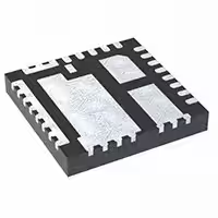
- Part No.:
- AOZ5038QI-05
- Manufacturer:
- Alpha & Omega Semiconductor Inc.
- Category:
- Power Driver Modules
- Package:
- 31-PowerVFQFN Module
- Datasheet:
-
 AOZ5038QI-05.pdf
- Description:
- MOD SYNC BUCK POWER STAGE 32QFN
- Quantity:
- Payment:

- Shipping:

Inventory:2,037
Please send an inquiry. Send us your inquiry, and we will respond immediately.
Product details
Overview
AOZ5038QI-05 from Alpha and Omega Semiconductor is a 50A continuous-current DrMOS power module integrating asymmetrical high-side and low-side MOSFETs with an on-die gate driver, optimized for synchronous buck conversion in VRMs. It supports 4.5V–25V input, delivers up to 60A peak current, operates up to 2MHz, and features integrated bootstrap Schottky diode and tri-state PWM compatibility for IMVP8/VRM13-compliant server and notebook CPU power delivery.
For engineers reviewing the AOZ5038QI-05 datasheet, pinout, applications, or equivalent options, key selection criteria include its 5mm × 5mm QFN-31L package with multi-VIN/VSWH/PGND terminals, FCCM-controlled diode emulation mode, UVLO thresholds (3.5V rising / 3.1V falling), and thermal resistance (RθJC = 2.5°C/W) for high-density point-of-load designs.
Technical Context
The AOZ5038QI-05 implements a dual-MOSFET synchronous buck stage with independently optimized devices: the high-side MOSFET prioritizes low gate charge and capacitance for fast switching at low duty cycles, while the low-side MOSFET minimizes RDS(ON) to reduce conduction loss. Its integrated driver supplies high peak current to GL and GH outputs with adaptive dead-time control based on VSWH and gate voltage monitoring.
Control logic includes tri-state PWM input (1.65V–3.5V window), FCCM pin enabling CCM (high), DCM/diode emulation (low), or full shutdown (floating), and internal UVLO with 500mV hysteresis. The module lacks built-in overcurrent or overtemperature protection-these functions must be implemented externally by the controller.
Key Specifications
| Parameter | Value and Actual Design Meaning |
|---|---|
| Continuous Output Current | 50A - Sustained load capability without derating under typical PCB thermal conditions (TA = 85°C, demo board). |
| Peak Output Current | 60A - Short-duration surge handling capacity before thermal or current-limiting constraints apply. |
| Input Voltage Range | 4.5V–25V - Supports wide-range DC inputs including 12V and 19V server rails and notebook adapters. |
| Switching Frequency | 200kHz–2MHz - Enables compact magnetics and high transient response in VRM applications. |
| Driver Supply (PVCC) | 4.5V–5.5V - Dedicated 5V rail required for low-side gate drive; decoupling capacitor must connect directly to PGND (Pin 28). |
| UVLO Threshold | 3.5V (rising), 3.1V (falling) - Ensures stable startup/shutdown sequencing; 500mV hysteresis prevents oscillation near threshold. |
| Thermal Resistance (Junction-to-Case) | 2.5°C/W - Enables direct thermal coupling to heatsink or copper plane; measured with PCB temp = 100°C. |
Pinout & Package
AOZ5038QI-05 uses a standard 5mm × 5mm QFN-31L package (QFN5x5_31L) with exposed thermal pad, RoHS-compliant, rated for –40°C to +85°C ambient operation. Pin layout is optimized for minimal parasitic inductance: VIN (Pins 8–11), PGND (Pins 12–15, 28), VSWH (Pins 7, 16–26), and dedicated BOOT (Pin 5) and GL (Pin 27, test-only) terminals.
| Pin/Terminal | Circuit Role | Design Meaning |
|---|---|---|
| PWM (Pin 1) | Logic-level control input | Accepts TTL-compatible 5V signals; tri-state window (1.65V–3.5V) enables safe high-impedance shutdown. |
| FCCM (Pin 2) | Mode-select control input | High = CCM operation; Low = diode emulation/skip mode; floating = full shutdown of both MOSFETs. |
| VCC (Pin 3) | Low-voltage driver supply | Supplies internal logic and level translators; requires 4.5V–7V, with UVLO at 3.5V rising. |
| BOOT (Pin 5) | High-side gate driver supply rail | Connects to bootstrap capacitor (100nF ceramic) between BOOT and VSWH (Pin 7); integrated Schottky diode eliminates external diode. |
| VSWH (Pins 7, 16–26) | Switching node | Common connection point for HS source and LS drain; used for bootstrap, zero-cross detection, UVLO, and anti-overlap control. |
| VIN (Pins 8–11) | High-voltage power input | Primary DC input path; multiple parallel pins minimize IR drop and inductance in high-current paths. |
| PGND (Pins 12–15, 28) | Power ground return | Dedicated low-inductance return for power stage and LS gate driver; Pin 28 is specifically for PVCC decoupling. |
| PVCC (Pin 29) | Low-side gate driver supply | 5V supply for LS gate drive circuitry; must be bypassed with ≥1µF ceramic cap directly to PGND (Pin 28). |
| GL (Pin 27) | Low-side gate monitor | Test-only terminal; not connected to internal LS gate pad; voltage measurement does not reflect actual gate drive waveform. |
Key Features
| Feature | Design Value |
|---|---|
| Integrated bootstrap Schottky diode | Eliminates external diode component and associated layout complexity while maintaining fast bootstrap recharge. |
| Tri-state PWM input compatibility | Enables seamless integration with digital controllers that support high-impedance PWM disable, reducing system-level sequencing overhead. |
| FCCM pin for multi-mode operation | Single-pin control of CCM, DCM, and diode emulation modes-critical for light-load efficiency optimization in VRMs. |
| Adaptive dead-time control | Monitors VSWH and gate voltages to dynamically adjust timing, preventing shoot-through across input bus under all operating conditions. |
| Optimized 5mm × 5mm QFN-31L layout | Groups VIN, PGND, and VSWH pins to minimize primary switching loop area, reducing EMI and voltage spikes at up to 2MHz operation. |
Applications
| Server VRMs | Notebook CPU Power |
|---|---|
Use Scenario: High-efficiency, high-current voltage regulation for dual-socket Xeon or EPYC processors in 1U/2U rack servers. IC Role / Device Role / Timing Role: DrMOS power stage delivering 50A continuous current per phase in multiphase IMVP8-compliant VRMs. Use Value: Enables >92% efficiency at 1V/50A output with 12V input, minimizing heat density and simplifying thermal management in constrained chassis space. | Use Scenario: Compact, high-transient-response power delivery for mobile Intel Core i7/i9 CPUs in ultrabooks and gaming laptops. IC Role / Device Role / Timing Role: Single-phase or multiphase buck stage supporting dynamic frequency scaling and rapid load steps up to 30A/µs. Use Value: 2MHz switching capability allows use of sub-300nH inductors and <1000µF total output capacitance, saving board area and cost. |
| Graphics Card VRMs | Memory Module PDNs |
Use Scenario: Multi-phase power delivery for NVIDIA RTX or AMD Radeon GPU cores requiring tight voltage tolerance (<±10mV) and fast transient recovery. IC Role / Device Role / Timing Role: High-current DrMOS stage synchronized with GPU controller to maintain precise VDDC regulation during burst workloads. Use Value: Ultra-low RDS(ON) low-side MOSFET and fast gate drive reduce conduction loss and improve transient droop performance. | Use Scenario: Point-of-load regulation for DDR4/DDR5 memory subsystems with strict noise and ripple requirements (e.g., <15mV p-p). IC Role / Device Role / Timing Role: Dedicated buck stage supplying 1.1V/1.2V to memory controllers and DRAM modules with minimal EMI impact on signal integrity. Use Value: Optimized pinout and integrated bootstrap diode suppress VSWH ringing, lowering conducted noise into adjacent high-speed data lanes. |
Equivalent & Alternatives
The following parts are listed as comparable options for similar DrMOS power stage applications.
| Alternative Part | Technical Difference | Application Difference | Selection Advice |
|---|---|---|---|
| IR35201MTRPBF | 60A continuous rating; supports 3.3V–25V VIN; requires external bootstrap diode; no integrated GL test pin. | Broadly compatible in IMVP8 systems but lacks tri-state PWM and diode emulation via FCCM pin. | Choose when higher current headroom is needed and external diode layout is acceptable. |
| TPS53679RTAT | 50A continuous; integrates PMBus interface and telemetry; requires external gate resistors; larger 6mm × 6mm QFN package. | Suitable for smart VRMs requiring real-time current/voltage reporting and programmable fault responses. | Choose when digital monitoring, configurability, and enhanced protection are required over analog simplicity. |
Compared with IR35201MTRPBF and TPS53679RTAT, the AOZ5038QI-05 offers superior integration (no external bootstrap diode), simpler analog control (single FCCM pin for mode selection), and smallest footprint (5mm × 5mm), making it optimal for space-constrained, cost-sensitive VRMs where digital telemetry is unnecessary.
Availability
AOZ5038QI-05 is available at Aetrix Electronics and suitable for server VRMs, notebook CPU power delivery, graphics card voltage regulation, and memory module point-of-load converters requiring stable component supply, long-term lifecycle support, and consistent parametric performance across production batches.
Supply support for AOZ5038QI-05 includes scheduled delivery planning, volume procurement assistance, BOM continuity management, traceable sourcing, and lifecycle availability coordination for OEM customers, industrial embedded developers, connected-device designers, and electronics production programs.
Manufacturer
Alpha and Omega Semiconductor (AOS) is a fabless power semiconductor company specializing in high-performance MOSFETs, IGBTs, and integrated power solutions for computing, consumer, and industrial markets.
The AOZ5038QI-05 belongs to AOS's DrMOS product line, designed specifically to meet IMVP8/VRM13 specifications for high-efficiency, high-current CPU and GPU power delivery in next-generation computing platforms.
FAQ
What is the maximum allowable input voltage for AOZ5038QI-05?
The AOZ5038QI-05 supports a recommended operating input voltage range of 4.5V to 25V. Its absolute maximum rating for VIN is 30V for transients ≤10ns per switching cycle. Exceeding 25V continuously may cause reliability degradation or exceed thermal limits under full load, so operation within the recommended range is required for guaranteed performance and lifetime.
Does AOZ5038QI-05 include overcurrent or overtemperature protection?
No, the AOZ5038QI-05 does not integrate overcurrent, overtemperature, or short-circuit protection circuits. It relies entirely on external controller-level protection (e.g., current-sense amplifiers, thermal monitors, and fault signaling via PWM/FCCM). The AOZ5038QI-05 only provides UVLO (3.5V rising) and shoot-through prevention via adaptive dead-time control.
Can AOZ5038QI-05 operate without an external bootstrap capacitor?
No, AOZ5038QI-05 requires an external 100nF ceramic capacitor connected between BOOT (Pin 5) and VSWH (Pin 7). Although the bootstrap Schottky diode is integrated, the capacitor is essential for sustaining high-side gate drive voltage during continuous conduction. Omitting it will result in high-side FET failure due to insufficient gate bias.
What is the function of the GL pin on AOZ5038QI-05?
The GL pin (Pin 27) on AOZ5038QI-05 is a low-side gate monitor terminal intended solely for factory functional testing. It is not directly connected to the internal low-side MOSFET gate pad, and its voltage waveform does not represent the actual gate drive signal. Designers must not connect external circuitry to GL in end applications.
Is AOZ5038QI-05 compliant with IMVP8 and VRM13 standards?
Yes, the AOZ5038QI-05 is fully compliant with Intel IMVP8 and VRM13 specifications in form, fit, and function. It meets timing, electrical, and thermal requirements for DrMOS power stages-including tri-state PWM compatibility, FCCM-controlled diode emulation, and 2MHz switching capability-making it suitable for certified motherboard and server VRM designs.
AOZ5038QI-05 Specifications
- Product attributes
- Attribute value
- Manufacturer:
- Alpha & Omega Semiconductor Inc.
- Series:
- -
- Package/Case:
- 31-PowerVFQFN Module
- Packaging:
- Tape & Reel (TR)
- Product Status:
- Not For New Designs
- Type:
- MOSFET
- Configuration:
- 1 Phase
- Current:
- 50 A
- Voltage:
- -
- Voltage - Isolation:
- -
- Grade:
- -
- Qualification:
- -
- Mounting Type:
- Surface Mount
AOZ5038QI-05 FAQ
1.How can I place an order for AOZ5038QI-05 through Aetrix?
Please submit a Request for Quotation (RFQ) for AOZ5038QI-05 on Aetrix. Our sales agent will provide a competitive quotation and guide you through the order confirmation once you accept the terms.
2.Are the price and stock information for AOZ5038QI-05 reliable?
The price and inventory of AOZ5038QI-05 are updated periodically and may fluctuate due to market conditions. Stock and pricing data are typically refreshed every 24 hours. Quotation validity for AOZ5038QI-05 is usually 5 days.
3.What payment methods are accepted for AOZ5038QI-05?
We accept Wire Transfer, PayPal, Credit Card, Western Union, MoneyGram, and Escrow for AOZ5038QI-05 transactions.
Note: Certain payment methods may incur a processing fee.
4.How is shipping managed for AOZ5038QI-05?
AOZ5038QI-05 orders can be shipped via leading logistics carriers, including DHL, UPS, FedEx, TNT, or Registered Mail.
Once your AOZ5038QI-05 order is processed, you will receive an email with the shipment details and tracking number.
Note: Tracking information may take up to 24 hours to appear. Express delivery typically takes 3–5 business days.
5.How can I obtain technical support or documentation for AOZ5038QI-05?
For technical support, including AOZ5038QI-05 datasheets, pinout diagrams, or application guidance, please contact our engineering support team. They can provide detailed documentation and assistance for your AOZ5038QI-05 requirements.
6.How does Aetrix verify that AOZ5038QI-05 is sourced from the original manufacturer or authorized distributors?
All AOZ5038QI-05 products on Aetrix are procured from qualified distributors and authorized channels. Our dedicated quality assurance team conducts strict verification, including traceability checks and, if necessary, third-party testing. This ensures that AOZ5038QI-05 meets industry standards.
7.What is the process for return or replacement of AOZ5038QI-05?
All AOZ5038QI-05 units undergo pre-shipment inspection (PSI). If there is an issue with AOZ5038QI-05, returns or replacements are accepted under the following conditions:
1.Quantity discrepancies, incorrect items, or visible external defects (such as breakage or corrosion), acknowledged by Aetrix.
2.The issue is reported within 90 days of delivery.
3.The AOZ5038QI-05 part is unused and in its original packaging.
Return procedure for AOZ5038QI-05:
1.Submit a request within 90 days.
2.Obtain a Return Material Authorization (RMA) from Aetrix.
AOZ5038QI-05 Tags
-
IGCM15F60GAXKMA1
Infineon Technologies
-
FSBB30CH60C
onsemi

-
LMG3522R030RQSR
Texas Instruments
-
LMG3522R030QRQSTQ1
Texas Instruments
-
IM828XCCXKMA1
Infineon Technologies
-
2SP0430T2A0C-FF1800R17IP5
Power Integrations
.jpg)
-
FBS-GAM02-P-C50
EPC Space, LLC
-
AOZ5507QI_2
Alpha & Omega Semiconductor Inc.
-
AOZ5517QI_2
Alpha & Omega Semiconductor Inc.
-
NV6117-RA
Navitas Semiconductor, Inc.
-
FDMF5062
onsemi
-
NV6127
Navitas Semiconductor, Inc.
Tech Hub

A practical engineering and sourcing framework covering lifecycle verification, lifetime-buy calculations, replacement qualification, supplier checks and counterfeit-risk controls.

TTL and CMOS logic families differ in thresholds, loading, output drive, power and timing. This engineering guide compares 74HC and 74HCT, calculates noise margins and checks 3.3 V/5 V compatibility.

A practical engineering guide to 3.3V and 5V logic compatibility, input thresholds, resistor dividers, translator ICs, MOSFET level shifting, I2C pull-ups, timing limits and power-sequencing risks.

The 74HC595 uses push-pull logic outputs, while the TPIC6B595 uses 50 V open-drain DMOS sinks for higher-power loads. This guide compares timing, current limits, 3.3 V interfacing, load wiring, thermal…

The 74HC595 converts serial data into eight stable parallel outputs. This guide covers pin functions, shift and storage timing, OE and MR behavior, drive-current limits, cascading, voltage compatibilit…

A technical comparison of level-sensitive latches and edge-triggered flip-flops, covering timing windows, setup and hold limits, master–slave operation, time borrowing, race-through, HDL inference and…

A D latch stores one bit while Enable controls when data can pass. This reference covers gate-level operation, truth tables, transparency, setup and hold timing, LE versus OE, common ICs and practical …

An SR latch stores one bit through cross-coupled feedback. This engineering reference covers NOR and NAND implementations, truth tables, forbidden-state recovery, gated operation, switch debouncing, fa…

Latch circuits retain one bit through feedback. This technical reference covers SR and D latches, truth tables, transparency, timing limits, latch-versus-flip-flop behavior, applications and common log…

An engineering guide to LED driver operation, constant-current and constant-voltage outputs, linear and switching topologies, dimming, IC selection, calculations, replacement compatibility, and fault c…


