
 My Inquiry
 My Account


NXP Semiconductors ASC8849AETE
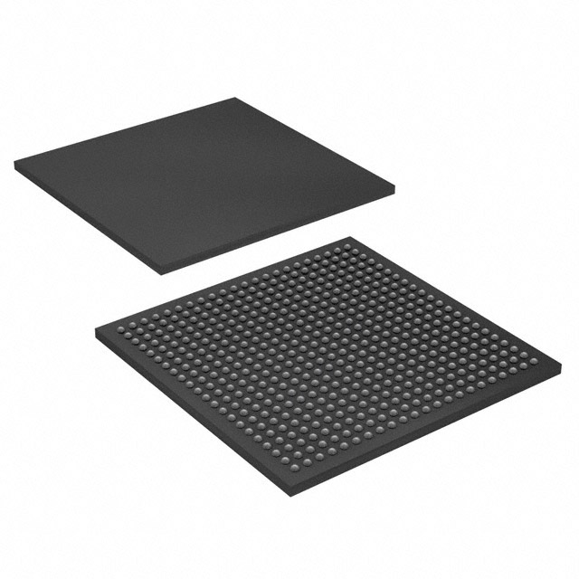
- Part No.:
- ASC8849AETE
- Manufacturer:
- NXP Semiconductors
- Category:
- Application Specific Microcontrollers
- Package:
- 484-TFBGA
- Datasheet:
-
 ASC8849AETE.pdf
- Description:
- IC VIDEO PROCESSOR ADV 484TFBGA
- Quantity:
- Payment:

- Shipping:

Inventory:4,029
Please send an inquiry. Send us your inquiry, and we will respond immediately.
Product details
Overview
ASC8849AETE from NXP Semiconductors is a high-performance IP camera SoC integrating ARM926EJ-S CPU (600 MHz), 12 MPixel sensor interface, dual hardware H.264/MJPEG encoders, and 24-bit RGB video output supporting 1080p @ 60 fps. It delivers full HD surveillance encoding with ROI, SVC-T, and intelligent video analytics including motion detection across 16 windows.
For engineers reviewing the ASC8849AETE datasheet, ASC8849AETE pinout, ASC8849AETE application, or ASC8849AETE equivalent, key selection criteria include its 12 MPixel raw input capability, dual-stream encoding (e.g., 1080p H.264 @ 35 fps + 1080p MJPEG @ 45 fps), 2-channel DDR-III memory controller, and TFBGA-484 package compatibility within the ASC884x/885x family.
Technical Context
This SoC implements a complete IP camera signal chain: raw Bayer/CMYG sensor data ingestion via 16-bit parallel interface (up to 180 MHz pixel clock), real-time ISP with 3D noise reduction, motion-adaptive de-interlacing, and digital WDR, followed by parallel H.264 High Profile (CAVLC/CABAC) and MJPEG baseline encoding engines.
It integrates a 600 MHz ARM926EJ-S core with 16 KB I/D cache, dual 16-bit DDR-III channels (up to 2 GB total), five I2S audio interfaces, MII/GMII/RGMII Ethernet MAC, USB 2.0 OTG, PCIe 1.1, and hardware-accelerated AES/SHA encryption - all synchronized under a unified clocking and power management architecture.
Key Specifications
| Parameter | Value and Actual Design Meaning |
|---|---|
| ARM CPU | ARM926EJ-S core at 600 MHz with 16 KB I-cache and 16 KB D-cache |
| Max Sensor Resolution | 12 MPixel raw input (16-bit Bayer/CMYG) with pixel clock up to 180 MHz |
| H.264 Encoding | High Profile up to 1080p @ 35 fps or 7×D1 @ 30 fps; supports ROI, SVC-T, 2 reference frames |
| MJPEG Encoding | Baseline profile up to 1080p @ 45 fps, independent of H.264 engine |
| Video Output | 24-bit RGB supporting 1080p @ 60 fps; also BT.1120 and BT.656 outputs |
| Memory Interface | Dual 16-bit DDR-III channels, each supporting up to 1 GB @ 400 MHz (2 GB total) |
| Package | TFBGA-484, 15 mm × 15 mm, 0.65 mm pitch |
Pinout & Package
ASC8849AETE is housed in a compact TFBGA-484 package (15 × 15 mm, 0.65 mm pitch) with 484 I/O balls arranged in a 22 × 22 array. Pin functions are defined per the ASC884xA/885xA family pinout specification; ball assignments support dedicated high-speed interfaces including DDR-III, BT.1120, PCIe, GMII, and multiple I2S lanes.
| Pin/Terminal | Circuit Role | Design Meaning |
|---|---|---|
| VDD_DDR | DDR memory I/O supply | 1.5 V (DDR-III) or 1.8 V (DDR-II) regulated supply for dual-channel memory interface |
| CLK_DDR | DDR clock input | Differential DDR clock pair (CLK_DDR_P/N) operating up to 400 MHz for 2× data rate |
| DATA[31:0] | DDR data bus | Two independent 16-bit bidirectional data buses (DDR_A[15:0], DDR_B[15:0]) |
| BT1120_D[23:0] | BT.1120 video data | 24-bit parallel YCbCr 4:2:2 interface supporting 1080p @ 60 fps input/output |
| I2S0_SDIN | I2S audio input | Primary I2S channel for stereo audio capture (left/right aligned, MSB-first) |
| GMII_TXD[7:0] | Gigabit Ethernet transmit | 8-bit GMII data bus for 1000BASE-T operation; requires external PHY |
Key Features
| Feature | Design Value |
|---|---|
| Dual hardware encoders | Independent H.264 High Profile and MJPEG baseline engines enabling true simultaneous multi-stream encoding without CPU load |
| Intelligent video analytics | Motion detection across 16 configurable windows, virtual fence, boundary control, and privacy masking implemented in hardware |
| Advanced ISP pipeline | Real-time 3D noise reduction, motion-adaptive de-interlacing, digital WDR, and photometric/geometric lens correction |
| Secure transmission | On-chip AES-128/192/256, SHA-224/256/384/512, and TDES acceleration for encrypted video streaming |
| Flexible sensor interfacing | Supports 16-bit raw CMOS sensors (Bayer/CMYG), BT.656 (8-channel), BT.1120, BT.601, and HDMI/HD-SDI receivers |
Applications
| Surveillance IP Cameras | Car Video Recorders |
|---|---|
Use Scenario: Outdoor fixed-mount or PTZ cameras requiring low-bitrate 1080p streaming over constrained bandwidth networks. IC Role / Device Role / Timing Role: Primary SoC handling sensor interface, ISP, dual-stream H.264/MJPEG encoding, Ethernet MAC, and secure transmission. Use Value: Enables 1080p @ 35 fps H.264 + 1080p @ 45 fps MJPEG substream with ROI-based bitrate optimization and hardware encryption. | Use Scenario: In-vehicle dashcams capturing high-resolution footage with motion-triggered recording and tamper-proof storage. IC Role / Device Role / Timing Role: Central processing unit managing wide-dynamic-range imaging, G-sensor integration via GPIO, and dual SD card recording with AES-encrypted video files. Use Value: Delivers 12 MPixel still capture and 1080p @ 60 fps local display while maintaining <1.5 W power consumption during continuous recording. |
| Digital Video Recorders (8×D1) | Industrial Vision Systems |
Use Scenario: Embedded DVRs aggregating video from eight analog cameras via BT.656 decoders and compressing to network storage. IC Role / Device Role / Timing Role: Multi-channel video processor accepting 8× BT.656 inputs, performing scaling, de-interlacing, and parallel H.264 encoding of all streams. Use Value: Achieves 8× D1 @ 30 fps H.264 compression using dedicated hardware engines, freeing ARM926EJ-S for metadata tagging and network protocol stack. | Use Scenario: Factory-floor inspection systems requiring precise color fidelity, geometric correction, and real-time defect detection. IC Role / Device Role / Timing Role: Vision coprocessor executing gamma correction, 12-bit per-channel LUTs, R/G/B histograms, and lens distortion compensation before analysis. Use Value: Provides calibrated 24-bit RGB output at 1080p @ 60 fps with independent black clamp and 64-bin histograms for statistical process control. |
Equivalent & Alternatives
The following parts are listed as comparable options for similar IP camera SoC applications.
| Alternative Part | Technical Difference | Application Difference | Selection Advice |
|---|---|---|---|
| ASC8850AETE | Same 12 MPixel sensor support and 600 MHz ARM926EJ-S, but adds PCIe 1.1 interface and enhanced Ethernet (RGMII) | Better suited for systems requiring host CPU offload via PCIe or gigabit Ethernet with reduced MAC overhead | Select ASC8850AETE when PCIe connectivity or RGMII PHY integration is required; otherwise ASC8849AETE offers identical imaging and encoding performance at lower BOM cost |
| ASC8848AETE | Lower 400 MHz ARM926EJ-S clock, 5 MPixel max sensor support, single DDR channel, and MII-only Ethernet | Targeted at cost-sensitive 720p/1080p @ 20–25 fps applications without multi-stream or high-resolution analytics | Choose ASC8848AETE only for entry-level IP cameras where 12 MPixel input, dual DDR, or 1080p @ 35 fps H.264 are not required |
Compared with ASC8848AETE and ASC8850AETE, ASC8849AETE provides optimal balance of 12 MPixel imaging capability, dual DDR-III bandwidth, and full H.264 High Profile encoding at 1080p @ 35 fps - making it ideal for mid-tier HD surveillance designs needing robust ISP and multi-stream flexibility without PCIe complexity.
Availability
ASC8849AETE is available at Aetrix Electronics and suitable for surveillance IP cameras, car video recorders, and industrial vision systems requiring stable component supply, long-term lifecycle support, and verified pin-compatible upgrades from legacy NXP camera SoCs.
Supply support for ASC8849AETE includes scheduled delivery planning, volume procurement assistance, BOM continuity management, traceable sourcing, and lifecycle availability coordination for OEM customers, industrial embedded developers, connected-device designers, and electronics production programs.
Manufacturer
NXP Semiconductors is a global semiconductor company headquartered in Eindhoven, Netherlands, specializing in secure connectivity solutions for automotive, industrial, and IoT applications.
The ASC884x/885x family was designed specifically for high-definition IP camera systems, integrating sensor interface, ISP, multi-standard video encoding, networking, and security into a single SoC to accelerate time-to-market for OEM camera manufacturers.
FAQ
What is the maximum sensor resolution supported by ASC8849AETE?
The ASC8849AETE supports up to 12 MPixel raw image sensors via its 16-bit parallel interface with pixel clock up to 180 MHz. This enables direct connection to high-resolution CMOS sensors in Bayer or CMYG format, and is confirmed in the ASC884xA/885xA selection guide and technical specifications document. The ASC8849AETE maintains full ISP and encoding functionality at this resolution, including 3D noise reduction and H.264 High Profile compression.
Does ASC8849AETE support both H.264 and MJPEG encoding simultaneously?
Yes, ASC8849AETE features independent hardware H.264 High Profile and MJPEG baseline encoding engines. It can encode, for example, a primary 1080p H.264 stream at 35 fps while simultaneously generating a 1080p MJPEG substream at 45 fps - confirmed in the product feature table and key benefits section. This dual-engine architecture eliminates CPU involvement in compression tasks.
What memory types and capacities does ASC8849AETE support?
ASC8849AETE integrates two 16-bit SDRAM channels supporting DDR-II (up to 512 MB per channel) or DDR-III (up to 1 GB per channel), for a total of 2 GB. The memory controller operates at up to 400 MHz, and the ASC8849AETE datasheet specifies timing compliance with JEDEC DDR-III standards. This configuration enables high-bandwidth video buffering for multi-stream encoding and ISP pipelines.
Is ASC8849AETE pin-compatible with other members of the ASC884x/885x family?
Yes, ASC8849AETE is fully pin-to-pin compatible with ASC8848AETE, ASC8850AETE, ASC8851AETE, and ASC8852AETE. This compatibility is explicitly stated in the official NXP documentation and enables hardware design reuse across resolutions and performance tiers. No PCB layout changes are required when upgrading from ASC8848AETE to ASC8849AETE or ASC8850AETE.
What video output interfaces does ASC8849AETE provide?
ASC8849AETE provides three primary video output paths: 24-bit RGB supporting 1080p @ 60 fps, BT.1120 supporting 1080p @ 60 fps, and BT.656 supporting 8-bit output. These are documented in the block diagram and selection guide. The 24-bit RGB interface is commonly used for direct connection to HDMI transmitters or LCD controllers in local display applications.
ASC8849AETE Specifications
- Product attributes
- Attribute value
- Manufacturer:
- NXP Semiconductors
- Series:
- -
- Package/Case:
- 484-TFBGA
- Packaging:
- Tray
- Product Status:
- Obsolete
- Programmable:
- Not Verified
- Applications:
- Embedded Multimedia Communication, Security and Entertainment
- Core Processor:
- ARM9®
- Program Memory Type:
- -
- Controller Series:
- -
- RAM Size:
- -
- Interface:
- EBI/EMI, Ethernet, I2S, IrDA, SD/MMC, SPI, UART/USART, USB OTG
- Number of I/O:
- -
- Voltage - Supply:
- -
- Operating Temperature:
- -
- Grade:
- -
- Qualification:
- -
- Mounting Type:
- Surface Mount
- Supplier Device Package:
- 484-TFBGA (15x15)
ASC8849AETE FAQ
1.How can I place an order for ASC8849AETE through Aetrix?
Please submit a Request for Quotation (RFQ) for ASC8849AETE on Aetrix. Our sales agent will provide a competitive quotation and guide you through the order confirmation once you accept the terms.
2.Are the price and stock information for ASC8849AETE reliable?
The price and inventory of ASC8849AETE are updated periodically and may fluctuate due to market conditions. Stock and pricing data are typically refreshed every 24 hours. Quotation validity for ASC8849AETE is usually 5 days.
3.What payment methods are accepted for ASC8849AETE?
We accept Wire Transfer, PayPal, Credit Card, Western Union, MoneyGram, and Escrow for ASC8849AETE transactions.
Note: Certain payment methods may incur a processing fee.
4.How is shipping managed for ASC8849AETE?
ASC8849AETE orders can be shipped via leading logistics carriers, including DHL, UPS, FedEx, TNT, or Registered Mail.
Once your ASC8849AETE order is processed, you will receive an email with the shipment details and tracking number.
Note: Tracking information may take up to 24 hours to appear. Express delivery typically takes 3–5 business days.
5.How can I obtain technical support or documentation for ASC8849AETE?
For technical support, including ASC8849AETE datasheets, pinout diagrams, or application guidance, please contact our engineering support team. They can provide detailed documentation and assistance for your ASC8849AETE requirements.
6.How does Aetrix verify that ASC8849AETE is sourced from the original manufacturer or authorized distributors?
All ASC8849AETE products on Aetrix are procured from qualified distributors and authorized channels. Our dedicated quality assurance team conducts strict verification, including traceability checks and, if necessary, third-party testing. This ensures that ASC8849AETE meets industry standards.
7.What is the process for return or replacement of ASC8849AETE?
All ASC8849AETE units undergo pre-shipment inspection (PSI). If there is an issue with ASC8849AETE, returns or replacements are accepted under the following conditions:
1.Quantity discrepancies, incorrect items, or visible external defects (such as breakage or corrosion), acknowledged by Aetrix.
2.The issue is reported within 90 days of delivery.
3.The ASC8849AETE part is unused and in its original packaging.
Return procedure for ASC8849AETE:
1.Submit a request within 90 days.
2.Obtain a Return Material Authorization (RMA) from Aetrix.
ASC8849AETE Tags

-
CYPD3175-24LQXQ
Infineon Technologies

-
SLB9672VU20FW1523XTMA1
Infineon Technologies

-
SLB9670VQ20FW785XTMA1
Infineon Technologies
-
SLB9672XU20FW1523XTMA1
Infineon Technologies
-
SLB9673XU20FW2613XTMA1
Infineon Technologies

-
CYPD3125-40LQXIT
Infineon Technologies

-
AT97SC3204-U2A1A-20
Microchip Technology
-
AT97SC3204-U2A1A-10
Microchip Technology
-
SLM9670AQ20FW1311XTMA1
Infineon Technologies
-
SLB9672XU20FW1613XTMA1
Infineon Technologies
-
SLB9672AU20FW1613XTMA1
Infineon Technologies
-
SLB9673AU20FW2613XTMA1
Infineon Technologies
Tech Hub

A practical engineering guide to 3.3V and 5V logic compatibility, input thresholds, resistor dividers, translator ICs, MOSFET level shifting, I2C pull-ups, timing limits and power-sequencing risks.

The 74HC595 uses push-pull logic outputs, while the TPIC6B595 uses 50 V open-drain DMOS sinks for higher-power loads. This guide compares timing, current limits, 3.3 V interfacing, load wiring, thermal…

The 74HC595 converts serial data into eight stable parallel outputs. This guide covers pin functions, shift and storage timing, OE and MR behavior, drive-current limits, cascading, voltage compatibilit…

A technical comparison of level-sensitive latches and edge-triggered flip-flops, covering timing windows, setup and hold limits, master–slave operation, time borrowing, race-through, HDL inference and…

A D latch stores one bit while Enable controls when data can pass. This reference covers gate-level operation, truth tables, transparency, setup and hold timing, LE versus OE, common ICs and practical …

An SR latch stores one bit through cross-coupled feedback. This engineering reference covers NOR and NAND implementations, truth tables, forbidden-state recovery, gated operation, switch debouncing, fa…

Latch circuits retain one bit through feedback. This technical reference covers SR and D latches, truth tables, transparency, timing limits, latch-versus-flip-flop behavior, applications and common log…

An engineering guide to LED driver operation, constant-current and constant-voltage outputs, linear and switching topologies, dimming, IC selection, calculations, replacement compatibility, and fault c…

Operational amplifier guide covering op amp basics, feedback, ideal vs real op amps, common configurations, buffer circuits, offset, bias current, gain-bandwidth, slew rate, rail-to-rail limits and sel…

Jumper cables guide covering safe connection order, red and black clamp placement, final ground connection, cable gauge, length, clamp quality, copper vs CCA cables, jump starter comparison and battery…


