
 My Inquiry
 My Account


NXP Semiconductors ASC8851AETE
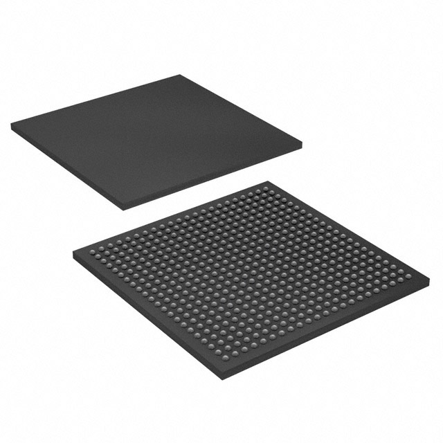
- Part No.:
- ASC8851AETE
- Manufacturer:
- NXP Semiconductors
- Category:
- Application Specific Microcontrollers
- Package:
- 484-TFBGA
- Datasheet:
-
 ASC8851AETE.pdf
- Description:
- IC VIDEO PROCESSOR ADV 484TFBGA
- Quantity:
- Payment:

- Shipping:

Inventory:4,017
Please send an inquiry. Send us your inquiry, and we will respond immediately.
Product details
Overview
ASC8851AETE from NXP Semiconductors is a high-performance IP camera SoC integrating ARM926EJ-S CPU (600 MHz), dual-channel DDR-II/III controller (2 × 16-bit, up to 2 GB total), and parallel H.264 High Profile + MJPEG hardware encoders. It supports 12 MPixel raw sensor input, 1080p@45 fps H.264 main stream + 1080p@45 fps MJPEG substream, and 24-bit RGB video output at 1080p@60 fps - deployed in HD surveillance cameras requiring low-bitrate, multi-stream encoding with motion detection and encryption.
For engineers reviewing the ASC8851AETE datasheet, ASC8851AETE pinout, ASC8851AETE application, or ASC8851AETE equivalent, key selection criteria include its 600 MHz ARM926EJ-S core, dual DDR-III channels, BT.1120/BT.656 video I/O support, five I2S interfaces, and AES/SHA-256 data encryption for secure video streaming in OEM camera designs.
Technical Context
This SoC implements a full imaging pipeline: raw Bayer/CMYG 16-bit sensor interface (up to 180 MHz pixel clock), 3D noise reduction, motion-adaptive de-interlacing, digital WDR, and photometric lens correction. Its dual independent compression engines enable simultaneous H.264 High Profile (CAVLC/CABAC) and MJPEG encoding with ROI and SVC-T support.
The integrated 10/100/1000 Ethernet MAC (MII/GMII/RGMII), USB 2.0 OTG, PCIe 1.1, and four full UARTs provide robust connectivity for PTZ control, SD card storage, NAND flash boot, and remote firmware updates - all coordinated by Linux 2.6 running on the cache-enabled ARM926EJ-S core.
Key Specifications
| Parameter | Value and Actual Design Meaning |
|---|---|
| ARM CPU | ARM926EJ-S @ 600 MHz with 16 KB I-Cache and 16 KB D-Cache - enables real-time Linux-based video analytics and multi-threaded encoding tasks. |
| Video Input | 16-bit raw CMOS/CCD sensor interface (up to 12 MPixel, 180 MHz pixel clock); BT.656 (8-ch), BT.1120 (1-ch) - supports high-resolution multi-sensor or HD-SDI receiver configurations. |
| H.264 Encoding | High Profile up to 1080p@45 fps + parallel MJPEG up to 1080p@45 fps - delivers dual-stream HD video with scalable bitrate control (VBR/CBR/CVBR) and SVC-T temporal scalability. |
| Memory Interface | Dual 16-bit DDR-II/III channels @ 400 MHz (max 1 GB per channel) - provides 1.6 GB/s bandwidth for ISP, encoding, and OS operations without bottleneck. |
| Video Output | 24-bit RGB + BT.1120 + BT.656 outputs supporting 1080p@60 fps - directly drives HDMI Tx, HD-SDI transmitters, or LCD panels without external frame buffers. |
| Security | AES, TDES, DES, SHA-1/224/256/384/512 - enables encrypted video transport and secure boot for compliance with ONVIF Profile S and GDPR-aligned deployments. |
| Audio Interface | Five I2S channels (4-in + 1-in/out); G.711/AAC/G.726 codecs - supports multi-mic audio capture, echo cancellation, and local playback in video door phones and conferencing systems. |
Pinout & Package
Package: TFBGA-484 (15 mm × 15 mm, 0.65 mm pitch). Pinout validated per NXP document 9397 750 17379 (March 2013) and ASC885xA reference schematic.
| Pin/Terminal | Circuit Role | Design Meaning |
|---|---|---|
| VDD_CORE | Core power supply | 1.2 V ±3% for ARM926EJ-S and ISP logic - requires low-noise regulation and local decoupling. |
| DDR_DQ[15:0] | DDR data bus (channel A) | 16-bit bidirectional data path to first DDR-III chip - routed with matched length and controlled impedance (50 Ω). |
| CLKIN | Reference clock input | 27 MHz crystal or LVCMOS clock for PLL generation of video, CPU, and memory clocks - critical for BT.1120 timing compliance. |
| BT1120_DATA[19:0] | BT.1120 parallel video input | 20-bit YUV/RGB data bus supporting 1080p@60 - requires 1.8 V I/O voltage and tight skew control vs. BT1120_CLK. |
| I2S0_SDI | I2S channel 0 data input | Left/right audio sample input from microphone preamp - used with I2S0_BCLK/I2S0_WS for synchronized stereo capture. |
| ETH_MDIO | PHY management interface | Open-drain MDIO/MDC for configuring external 10/100/1000 PHY - enables auto-negotiation and link status monitoring. |
Key Features
| Feature | Design Value |
|---|---|
| Parallel H.264 + MJPEG encoding | Enables simultaneous main stream (1080p@45 fps H.264) and substream (1080p@45 fps MJPEG) without CPU load - reduces system latency and simplifies RTSP server design. |
| Motion detection (16 windows) | Hardware-accelerated pixel-level analysis per window - eliminates need for software-based OpenCV processing and lowers power in battery-powered car DVRs. |
| ROI encoding | Allows encoder to allocate higher bitrate to user-defined regions (e.g., faces, license plates) while compressing background at lower quality - improves forensic detail retention. |
| SVC-T temporal scalability | Generates multiple temporal layers (e.g., 1080p@30 + @15 + @7.5 fps) from single encode pass - supports adaptive streaming over variable-bandwidth networks without re-encoding. |
| Advanced ISP pipeline | Includes 3D noise reduction, motion-adaptive de-interlacing, and digital WDR - delivers clean, flicker-free 1080p video under low-light or high-contrast lighting without external processors. |
Applications
| Surveillance IP Cameras | Car Video Recorders |
|---|---|
Use Scenario: Outdoor dome camera capturing 1080p@45 fps video with motion-triggered recording and tamper detection. IC Role / Device Role / Timing Role: Primary SoC handling sensor interface, ISP, dual-stream H.264/MJPEG encoding, Ethernet transmission, and AES encryption. Use Value: 12 MPixel sensor support and ROI encoding preserve license plate clarity at night; <1.5 W power enables passive cooling in sealed enclosures. | Use Scenario: Dual-camera dashcam recording front and cabin views with GPS timestamping and emergency lock-on. IC Role / Device Role / Timing Role: Central video processor managing two BT.656 inputs, time-synchronized encoding, SD card write buffering, and CAN bus metadata injection. Use Value: Hardware motion detection across 16 windows triggers instant file protection; dual DDR-III channels sustain 1080p@30 fps write throughput to UHS-I SD cards. |
| Digital Video Recorders (8×D1) | Video Door Phones |
Use Scenario: 8-channel DVR aggregating video from analog cameras via BT.656 decoders and encoding to network storage. IC Role / Device Role / Timing Role: Multi-channel video ingest SoC accepting eight BT.656 streams, performing per-channel H.264 compression, and multiplexing over Gigabit Ethernet. Use Value: 8-channel BT.656 support eliminates need for external video switchers; RGMII interface sustains 8×D1@30 fps aggregate throughput (≈200 Mbps). | Use Scenario: HD intercom unit with 1080p camera, two-way audio, IR illumination, and door relay control. IC Role / Device Role / Timing Role: Integrated media processor handling video capture, MJPEG substream for mobile viewing, G.711 audio codec, and GPIO-driven IR-cut/relay sequencing. Use Value: Five I2S interfaces allow simultaneous mic input, speaker output, and audio loopback; 24-bit RGB output drives internal LCD with zero frame delay. |
Equivalent & Alternatives
The following parts are listed as comparable options for similar IP camera SoC applications.
| Alternative Part | Technical Difference | Application Difference | Selection Advice |
|---|---|---|---|
| ASC8850AETE | Same package and pinout; ARM926EJ-S @ 600 MHz but rated for 1080p@35 fps H.264 (vs. 45 fps for ASC8851AETE) | Lower max encoding throughput; suitable for cost-sensitive 1080p@30 fps fixed-focus cameras without SVC-T | Select ASC8850AETE when full 45 fps capability is unnecessary and BOM cost reduction is prioritized. |
| ASC8852AETE | Same package and pinout; supports 1080p@65 fps H.264 and 13×D1@30 fps - highest performance in ASC885xA family | Targeted at premium multi-sensor panoramic cameras requiring >45 fps sustained encoding and advanced lens correction | Choose ASC8852AETE for ultra-low-latency applications like industrial vision inspection where frame rate headroom is critical. |
Compared with ASC8850AETE and ASC8852AETE, the ASC8851AETE delivers optimal balance of 1080p@45 fps encoding, dual-stream flexibility, and power efficiency (<1.5 W), making it ideal for mainstream HD IP cameras where thermal envelope and cost constrain peak performance requirements.
Availability
ASC8851AETE is available at Aetrix Electronics and suitable for surveillance IP cameras, car video recorders, and video door phones requiring stable component supply, long-term lifecycle assurance, and traceable sourcing for industrial-grade deployments.
Supply support for ASC8851AETE includes scheduled delivery planning, volume procurement assistance, BOM continuity management, traceable sourcing, and lifecycle availability coordination for OEM customers, industrial embedded developers, connected-device designers, and electronics production programs.
Manufacturer
NXP Semiconductors is a global semiconductor company headquartered in Eindhoven, Netherlands, specializing in secure connectivity solutions for automotive, industrial, and IoT markets.
The ASC885xA family - including ASC8851AETE - was designed as a pin-compatible, software-upgradable evolution of NXP's IP camera SoC platform, targeting seamless migration from 720p to 1080p@60 systems with enhanced low-light ISP and hardware encryption.
FAQ
What video sensor interfaces does the ASC8851AETE support?
The ASC8851AETE supports 16-bit raw CMOS/CCD sensor input (Bayer/CMYG) up to 12 MPixel and 180 MHz pixel clock, plus standardized video interfaces including BT.656 (8-channel), BT.1120 (1-channel), and BT.601. These allow direct connection to image sensors or external decoders in ASC8851AETE-based camera designs without intermediate logic.
Does the ASC8851AETE include hardware encryption for secure video streaming?
Yes, the ASC8851AETE integrates dedicated cryptographic accelerators supporting AES, TDES, DES, and SHA-1/224/256/384/512. This enables end-to-end encrypted video transport compliant with ONVIF Profile S and enterprise security policies - a core capability built into the ASC8851AETE silicon, not dependent on software-only implementations.
What is the maximum H.264 encoding performance of the ASC8851AETE?
The ASC8851AETE achieves up to 1080p@45 fps H.264 High Profile encoding with CAVLC/CABAC entropy coding, two reference frames, ROI, and SVC-T. This is confirmed in NXP's ASC885xA selection guide and exceeds ASC8850AETE (35 fps) while falling short of ASC8852AETE (65 fps), positioning ASC8851AETE for mainstream HD camera applications.
How many DDR memory channels does the ASC8851AETE support, and what is the maximum capacity?
The ASC8851AETE supports two independent 16-bit DDR-II/III memory channels, each operating up to 400 MHz. Each channel supports up to 1 GB DDR-III or 512 MB DDR-II, enabling a total system memory capacity of up to 2 GB - sufficient for concurrent ISP, encoding, OS, and network stack operations in ASC8851AETE-based platforms.
Is the ASC8851AETE pin-to-pin compatible with other members of the ASC885xA family?
Yes, the ASC8851AETE is fully pin-to-pin and software-compatible with ASC8850AETE and ASC8852AETE in the TFBGA-484 package. This allows hardware reuse across performance tiers - for example, upgrading from ASC8850AETE to ASC8851AETE requires only firmware update and no PCB redesign, as confirmed in NXP's migration documentation.
ASC8851AETE Specifications
- Product attributes
- Attribute value
- Manufacturer:
- NXP Semiconductors
- Series:
- -
- Package/Case:
- 484-TFBGA
- Packaging:
- Tray
- Product Status:
- Obsolete
- Programmable:
- Not Verified
- Applications:
- Embedded Multimedia Communication, Security and Entertainment
- Core Processor:
- ARM9®
- Program Memory Type:
- -
- Controller Series:
- -
- RAM Size:
- -
- Interface:
- EBI/EMI, Ethernet, I2S, IrDA, SD/MMC, SPI, UART/USART, USB OTG
- Number of I/O:
- -
- Voltage - Supply:
- -
- Operating Temperature:
- -
- Grade:
- -
- Qualification:
- -
- Mounting Type:
- Surface Mount
- Supplier Device Package:
- 484-TFBGA (15x15)
ASC8851AETE FAQ
1.How can I place an order for ASC8851AETE through Aetrix?
Please submit a Request for Quotation (RFQ) for ASC8851AETE on Aetrix. Our sales agent will provide a competitive quotation and guide you through the order confirmation once you accept the terms.
2.Are the price and stock information for ASC8851AETE reliable?
The price and inventory of ASC8851AETE are updated periodically and may fluctuate due to market conditions. Stock and pricing data are typically refreshed every 24 hours. Quotation validity for ASC8851AETE is usually 5 days.
3.What payment methods are accepted for ASC8851AETE?
We accept Wire Transfer, PayPal, Credit Card, Western Union, MoneyGram, and Escrow for ASC8851AETE transactions.
Note: Certain payment methods may incur a processing fee.
4.How is shipping managed for ASC8851AETE?
ASC8851AETE orders can be shipped via leading logistics carriers, including DHL, UPS, FedEx, TNT, or Registered Mail.
Once your ASC8851AETE order is processed, you will receive an email with the shipment details and tracking number.
Note: Tracking information may take up to 24 hours to appear. Express delivery typically takes 3–5 business days.
5.How can I obtain technical support or documentation for ASC8851AETE?
For technical support, including ASC8851AETE datasheets, pinout diagrams, or application guidance, please contact our engineering support team. They can provide detailed documentation and assistance for your ASC8851AETE requirements.
6.How does Aetrix verify that ASC8851AETE is sourced from the original manufacturer or authorized distributors?
All ASC8851AETE products on Aetrix are procured from qualified distributors and authorized channels. Our dedicated quality assurance team conducts strict verification, including traceability checks and, if necessary, third-party testing. This ensures that ASC8851AETE meets industry standards.
7.What is the process for return or replacement of ASC8851AETE?
All ASC8851AETE units undergo pre-shipment inspection (PSI). If there is an issue with ASC8851AETE, returns or replacements are accepted under the following conditions:
1.Quantity discrepancies, incorrect items, or visible external defects (such as breakage or corrosion), acknowledged by Aetrix.
2.The issue is reported within 90 days of delivery.
3.The ASC8851AETE part is unused and in its original packaging.
Return procedure for ASC8851AETE:
1.Submit a request within 90 days.
2.Obtain a Return Material Authorization (RMA) from Aetrix.
ASC8851AETE Tags

-
CYPD3175-24LQXQ
Infineon Technologies

-
SLB9672VU20FW1523XTMA1
Infineon Technologies

-
SLB9670VQ20FW785XTMA1
Infineon Technologies
-
SLB9672XU20FW1523XTMA1
Infineon Technologies
-
SLB9673XU20FW2613XTMA1
Infineon Technologies

-
CYPD3125-40LQXIT
Infineon Technologies

-
AT97SC3204-U2A1A-20
Microchip Technology
-
AT97SC3204-U2A1A-10
Microchip Technology
-
SLM9670AQ20FW1311XTMA1
Infineon Technologies
-
SLB9672XU20FW1613XTMA1
Infineon Technologies
-
SLB9672AU20FW1613XTMA1
Infineon Technologies
-
SLB9673AU20FW2613XTMA1
Infineon Technologies
Tech Hub

A practical engineering guide to 3.3V and 5V logic compatibility, input thresholds, resistor dividers, translator ICs, MOSFET level shifting, I2C pull-ups, timing limits and power-sequencing risks.

The 74HC595 uses push-pull logic outputs, while the TPIC6B595 uses 50 V open-drain DMOS sinks for higher-power loads. This guide compares timing, current limits, 3.3 V interfacing, load wiring, thermal…

The 74HC595 converts serial data into eight stable parallel outputs. This guide covers pin functions, shift and storage timing, OE and MR behavior, drive-current limits, cascading, voltage compatibilit…

A technical comparison of level-sensitive latches and edge-triggered flip-flops, covering timing windows, setup and hold limits, master–slave operation, time borrowing, race-through, HDL inference and…

A D latch stores one bit while Enable controls when data can pass. This reference covers gate-level operation, truth tables, transparency, setup and hold timing, LE versus OE, common ICs and practical …

An SR latch stores one bit through cross-coupled feedback. This engineering reference covers NOR and NAND implementations, truth tables, forbidden-state recovery, gated operation, switch debouncing, fa…

Latch circuits retain one bit through feedback. This technical reference covers SR and D latches, truth tables, transparency, timing limits, latch-versus-flip-flop behavior, applications and common log…

An engineering guide to LED driver operation, constant-current and constant-voltage outputs, linear and switching topologies, dimming, IC selection, calculations, replacement compatibility, and fault c…

Operational amplifier guide covering op amp basics, feedback, ideal vs real op amps, common configurations, buffer circuits, offset, bias current, gain-bandwidth, slew rate, rail-to-rail limits and sel…

Jumper cables guide covering safe connection order, red and black clamp placement, final ground connection, cable gauge, length, clamp quality, copper vs CCA cables, jump starter comparison and battery…


