
 My Inquiry
 My Account


Nexperia USA Inc. BAW56S-QX
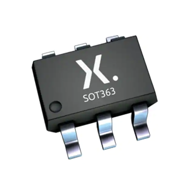
- Part No.:
- BAW56S-QX
- Manufacturer:
- Nexperia USA Inc.
- Category:
- Diode Arrays
- Package:
- 6-TSSOP, SC-88, SOT-363
- Datasheet:
-
 BAW56S-QX.pdf
- Description:
- DIODE ARRAY GP 90V 250MA 6-TSSOP
- Quantity:
- Payment:

- Shipping:

Inventory:2,732
Please send an inquiry. Send us your inquiry, and we will respond immediately.
Product details
Overview
BAW56S-Q from Nexperia is a dual-common-anode high-speed switching diode array in SOT363-3 (TSSOP6) package, comprising four diodes configured as two independent common-anode pairs (A1/A2–K1/K2 and A3/A4–K3/K4), with trr ≤ 4 ns, Cd ≤ 2 pF, VR = 90 V, and qualified per AEC-Q101 for automotive signal routing and clamping.
For engineers reviewing the BAW56S-Q datasheet, BAW56S-Q pinout, BAW56S-Q application, or BAW56S-Q equivalent, this device supports high-frequency digital signal steering, ESD-protected I/O buffering, and low-capacitance voltage clamping in space-constrained automotive ECUs and ADAS sensor interfaces.
Technical Context
The BAW56S-Q integrates four discrete high-speed diodes in a single 6-pin TSSOP package, arranged as two electrically isolated dual-diode structures sharing common anodes-enabling bidirectional clamping or dual-channel level translation without cross-talk. Its trr ≤ 4 ns and Cd ≤ 2 pF at 1 MHz support operation up to ~100 MHz in fast-switching logic interfaces.
Designed for automotive-grade reliability, it sustains IF = 250 mA per diode at Ts = 60 °C, operates across –65 °C to +150 °C ambient, and meets AEC-Q101 stress test requirements including HTGB, HTRB, and temperature cycling-ensuring robustness in engine control and infotainment power domains.
Key Specifications
| Parameter | Value and Actual Design Meaning |
|---|---|
| Reverse Voltage (VR) | 90 V - supports 24 V automotive supply rail transient suppression with 2× safety margin. |
| Reverse Recovery Time (trr) | ≤ 4 ns - enables clean switching in >100 MHz digital signal paths without tail current distortion. |
| Diode Capacitance (Cd) | ≤ 2 pF at 0 V, 1 MHz - minimizes signal loading on high-speed data lines (e.g., CAN FD, LIN, SPI). |
| Forward Voltage (VF) | 855 mV at IF = 10 mA - ensures low conduction loss in active clamping and logic-level shifting circuits. |
| Reverse Current (IR) | ≤ 0.5 µA at VR = 80 V, 25 °C - maintains high impedance isolation in standby and sleep-mode signal paths. |
| Junction Temperature (Tj) | 150 °C max - allows continuous operation in under-hood environments without derating at full current. |
Pinout & Package
Package: SOT363-3 (TSSOP6), 1.3 mm × 2.2 mm × 0.95 mm body, 0.65 mm lead pitch, surface-mount plastic package with exposed thermal pad not present.
| Pin/Terminal | Circuit Role | Design Meaning |
|---|---|---|
| 1 | K1 | Cathode of Diode 1 - connects to signal line requiring clamping toward common anode A1/A2. |
| 2 | K2 | Cathode of Diode 2 - forms second leg of first common-anode pair (A1/A2–K1/K2) for differential or redundant clamping. |
| 3 | A3/A4 | Common anode of Diodes 3 and 4 - provides shared positive reference for second independent dual-diode channel. |
| 4 | K3 | Cathode of Diode 3 - routes to secondary signal path (e.g., backup sensor input or alternate bus line). |
| 5 | K4 | Cathode of Diode 4 - completes second dual-diode structure, enabling independent bidirectional protection per channel. |
| 6 | A1/A2 | Common anode of Diodes 1 and 2 - ties to local VCC or bias rail for active clamping or level-shifting function. |
Key Features
| Feature | Design Value |
|---|---|
| High-speed switching | trr ≤ 4 ns enables use in 100+ MHz clock distribution and high-data-rate serial interface protection. |
| Low junction capacitance | Cd ≤ 2 pF preserves signal integrity on high-speed traces without added RC delay or reflection. |
| AEC-Q101 qualification | Validated for automotive under-hood applications including engine management and ADAS camera modules. |
| Dual common-anode topology | Two independent 2-diode groups allow separate clamping of two signal pairs using one footprint. |
| Thermal robustness | Rth(j-sp) = 255 K/W and Tj(max) = 150 °C support sustained operation in thermally dense PCB layouts. |
Applications
| Automotive CAN FD Transceiver Protection | High-Speed Digital I/O Clamping |
|---|---|
|
Use Scenario: Protecting CAN FD transceiver pins against ESD and load-dump transients in vehicle networking modules. IC Role / Device Role / Timing Role: Bidirectional voltage clamp placed between TX/RX lines and VCC/GND rails to limit excursion beyond safe logic thresholds. Use Value: 4 ns trr prevents latch-up during fast edge transitions; 2 pF capacitance avoids signal rise-time degradation on 5 Mbit/s CAN FD buses. |
Use Scenario: Shielding FPGA or MCU GPIOs from overvoltage events in industrial HMI panels and sensor hubs. IC Role / Device Role / Timing Role: Dual-channel rail-to-rail clamping diode array providing simultaneous protection for complementary signal pairs. Use Value: Independent A1/A2 and A3/A4 anodes allow separate biasing for pull-up and pull-down domains without interference. |
| ADAS Camera Interface Level Shifting | Automotive LIN Bus Signal Conditioning |
|
Use Scenario: Translating 1.8 V MIPI CSI-2 signals from image sensors to 3.3 V processor inputs in surround-view systems. IC Role / Device Role / Timing Role: Active clamping diode used in series with resistive divider to enforce precise voltage thresholds at receiver inputs. Use Value: Low VF (855 mV @ 10 mA) ensures minimal offset error; 90 V VR rating accommodates worst-case surge coupling. |
Use Scenario: Improving noise immunity on LIN bus master/slave nodes in body control modules and door modules. IC Role / Device Role / Timing Role: Common-anode dual-diode configuration used for bus-line pull-up stabilization and transient suppression. Use Value: 0.5 µA IR at 80 V ensures negligible leakage current in always-on LIN standby mode, preserving battery life. |
Equivalent & Alternatives
The following parts are listed as comparable options for similar high-speed switching diode array applications.
| Alternative Part | Technical Difference | Application Difference | Selection Advice |
|---|---|---|---|
| BAV99W-Q | Single common-cathode dual-diode (SOT323), trr = 4 ns, Cd = 2 pF, VR = 70 V, no AEC-Q101 qualification. | Limited to non-automotive consumer or industrial applications due to lower VR and lack of automotive qualification. | Select when cost sensitivity outweighs automotive compliance and 90 V VR headroom is unnecessary. |
| NSR0230P2T5G | Single Schottky diode (SOD-523), VF = 370 mV @ 200 mA, trr not specified (Schottky), VR = 30 V, AEC-Q101 qualified. | Not pin-compatible; lacks dual-diode topology and common-anode architecture required for paired signal protection. | Choose only for ultra-low VF requirements in low-voltage (<3.3 V) clamping where reverse recovery is irrelevant. |
Compared with BAV99W-Q and NSR0230P2T5G, the BAW56S-Q uniquely delivers AEC-Q101-compliant dual-channel common-anode switching in a compact 6-pin TSSOP, supporting higher VR, matched diode pairing, and true high-speed signal integrity-making it the sole fit for dual-rail automotive data interface protection.
Availability
BAW56S-Q is available at Aetrix Electronics and suitable for automotive electronic control units, ADAS camera modules, and high-speed industrial communication interfaces requiring stable component supply, long-term lifecycle assurance, and AEC-Q101-compliant sourcing.
Supply support for BAW56S-Q includes scheduled delivery planning, volume procurement assistance, BOM continuity management, traceable sourcing, and lifecycle availability coordination for OEM customers, industrial embedded developers, connected-device designers, and electronics production programs.
Manufacturer
Nexperia is a global semiconductor expert focused on essential efficiency technologies, delivering high-performance, reliable discrete, logic, and MOSFET solutions for automotive, industrial, and mobile markets.
The BAW56S-Q belongs to Nexperia's AEC-Q101-qualified high-speed diode portfolio, engineered specifically for signal integrity preservation and transient robustness in automotive data networks and sensor interfaces.
FAQ
What is the maximum continuous forward current per diode in the BAW56S-Q?
The BAW56S-Q supports a continuous forward current of 250 mA per diode at a solder-point temperature (Ts) of 60 °C, as defined in its limiting values table. This rating assumes mounting on a standard FR4 PCB with single-sided copper and tin-plated finish. Derating applies above Ts = 60 °C, with total power dissipation limited to 350 mW per device.
Can the BAW56S-Q be used for bidirectional ESD protection on a differential pair?
Yes-the BAW56S-Q's dual common-anode configuration allows each diode pair (e.g., A1/A2–K1/K2) to clamp one side of a differential signal to VCC, while the second pair (A3/A4–K3/K4) clamps the other side. With trr ≤ 4 ns and Cd ≤ 2 pF, it preserves signal symmetry and timing margins in USB 2.0, LVDS, or MIPI D-PHY interfaces without introducing skew.
Is the BAW56S-Q pin-compatible with the legacy BAW56S?
No-the BAW56S-Q uses the SOT363-3 (TSSOP6) package with updated pinning and AEC-Q101 qualification, whereas the legacy BAW56S was packaged in SOT363 (non–"-3" variant) with different mechanical tolerances and no automotive qualification. Footprint dimensions differ slightly, and the pin 3 / pin 6 anode assignments are redefined; PCB layout revision is required.
What is the thermal resistance from junction to solder point (Rth(j-sp)) for the BAW56S-Q?
The BAW56S-Q has a typical thermal resistance of 255 K/W from junction to solder point (Rth(j-sp)), measured on an FR4 PCB with standard single-sided copper and tin-plated finish. This value enables direct thermal modeling for board-level reliability analysis and confirms suitability for operation up to 150 °C junction temperature under defined power dissipation limits.
BAW56S-QX Specifications
- Product attributes
- Attribute value
- Manufacturer:
- Nexperia USA Inc.
- Series:
- -
- Package/Case:
- 6-TSSOP, SC-88, SOT-363
- Packaging:
- Tape & Reel (TR)
- Product Status:
- Active
- Diode Configuration:
- 2 Pair Common Anode
- Technology:
- Standard
- Voltage - DC Reverse (Vr) (Max):
- 90 V
- Current - Average Rectified (Io) (per Diode):
- 250mA (DC)
- Voltage - Forward (Vf) (Max) @ If:
- 1.25 V @ 150 mA
- Speed:
- Fast Recovery =< 500ns, > 200mA (Io)
- Reverse Recovery Time (trr):
- 4 ns
- Current - Reverse Leakage @ Vr:
- 500 nA @ 80 V
- Operating Temperature - Junction:
- 150°C
- Grade:
- Automotive
- Qualification:
- AEC-Q101
- Mounting Type:
- Surface Mount
- Supplier Device Package:
- 6-TSSOP
BAW56S-QX FAQ
1.How can I place an order for BAW56S-QX through Aetrix?
Please submit a Request for Quotation (RFQ) for BAW56S-QX on Aetrix. Our sales agent will provide a competitive quotation and guide you through the order confirmation once you accept the terms.
2.Are the price and stock information for BAW56S-QX reliable?
The price and inventory of BAW56S-QX are updated periodically and may fluctuate due to market conditions. Stock and pricing data are typically refreshed every 24 hours. Quotation validity for BAW56S-QX is usually 5 days.
3.What payment methods are accepted for BAW56S-QX?
We accept Wire Transfer, PayPal, Credit Card, Western Union, MoneyGram, and Escrow for BAW56S-QX transactions.
Note: Certain payment methods may incur a processing fee.
4.How is shipping managed for BAW56S-QX?
BAW56S-QX orders can be shipped via leading logistics carriers, including DHL, UPS, FedEx, TNT, or Registered Mail.
Once your BAW56S-QX order is processed, you will receive an email with the shipment details and tracking number.
Note: Tracking information may take up to 24 hours to appear. Express delivery typically takes 3–5 business days.
5.How can I obtain technical support or documentation for BAW56S-QX?
For technical support, including BAW56S-QX datasheets, pinout diagrams, or application guidance, please contact our engineering support team. They can provide detailed documentation and assistance for your BAW56S-QX requirements.
6.How does Aetrix verify that BAW56S-QX is sourced from the original manufacturer or authorized distributors?
All BAW56S-QX products on Aetrix are procured from qualified distributors and authorized channels. Our dedicated quality assurance team conducts strict verification, including traceability checks and, if necessary, third-party testing. This ensures that BAW56S-QX meets industry standards.
7.What is the process for return or replacement of BAW56S-QX?
All BAW56S-QX units undergo pre-shipment inspection (PSI). If there is an issue with BAW56S-QX, returns or replacements are accepted under the following conditions:
1.Quantity discrepancies, incorrect items, or visible external defects (such as breakage or corrosion), acknowledged by Aetrix.
2.The issue is reported within 90 days of delivery.
3.The BAW56S-QX part is unused and in its original packaging.
Return procedure for BAW56S-QX:
1.Submit a request within 90 days.
2.Obtain a Return Material Authorization (RMA) from Aetrix.
BAW56S-QX Tags
-
BAV99-7-F
Diodes Incorporated
-
BAT54C-7-F
Diodes Incorporated
-
BAV99,215
Nexperia USA Inc.
-
BAT54SLT1G
onsemi
-
BAV70LT1G
onsemi
-
BAT54CLT1G
onsemi
-
BAT54S-7-F
Diodes Incorporated
-
BAV99LT1G
onsemi
-
BAT54S,215
Nexperia USA Inc.
-
BAS40-04LT1G
onsemi
-
MMBD1503-TP
Micro Commercial Co
-
BAV99WT1G
onsemi
Tech Hub

A practical engineering guide to 3.3V and 5V logic compatibility, input thresholds, resistor dividers, translator ICs, MOSFET level shifting, I2C pull-ups, timing limits and power-sequencing risks.

The 74HC595 uses push-pull logic outputs, while the TPIC6B595 uses 50 V open-drain DMOS sinks for higher-power loads. This guide compares timing, current limits, 3.3 V interfacing, load wiring, thermal…

The 74HC595 converts serial data into eight stable parallel outputs. This guide covers pin functions, shift and storage timing, OE and MR behavior, drive-current limits, cascading, voltage compatibilit…

A technical comparison of level-sensitive latches and edge-triggered flip-flops, covering timing windows, setup and hold limits, master–slave operation, time borrowing, race-through, HDL inference and…

A D latch stores one bit while Enable controls when data can pass. This reference covers gate-level operation, truth tables, transparency, setup and hold timing, LE versus OE, common ICs and practical …

An SR latch stores one bit through cross-coupled feedback. This engineering reference covers NOR and NAND implementations, truth tables, forbidden-state recovery, gated operation, switch debouncing, fa…

Latch circuits retain one bit through feedback. This technical reference covers SR and D latches, truth tables, transparency, timing limits, latch-versus-flip-flop behavior, applications and common log…

An engineering guide to LED driver operation, constant-current and constant-voltage outputs, linear and switching topologies, dimming, IC selection, calculations, replacement compatibility, and fault c…

Operational amplifier guide covering op amp basics, feedback, ideal vs real op amps, common configurations, buffer circuits, offset, bias current, gain-bandwidth, slew rate, rail-to-rail limits and sel…

Jumper cables guide covering safe connection order, red and black clamp placement, final ground connection, cable gauge, length, clamp quality, copper vs CCA cables, jump starter comparison and battery…


