
 My Inquiry
 My Account


NXP Semiconductors BT131-600/DG,116
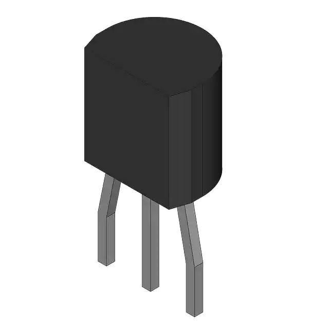
- Part No.:
- BT131-600/DG,116
- Manufacturer:
- NXP Semiconductors
- Category:
- TRIACs
- Package:
- TO-226-3, TO-92-3 (TO-226AA) Formed Leads
- Datasheet:
-
 BT131-600/DG,116.pdf
- Description:
- TRIAC SENS GATE 600V 1A TO92-3
- Quantity:
- Payment:

- Shipping:

Inventory:10,000
Please send an inquiry. Send us your inquiry, and we will respond immediately.
Product details
Overview
BT131-600/DG,116 from NXP Semiconductors is a passivated, sensitive-gate logic-level triac in SOT54 (TO-92) package, rated for 600 V repetitive peak off-state voltage (VDRM), 1 A RMS on-state current (IT(RMS)), and 12.5 A non-repetitive surge current (ITSM). It interfaces directly with microcontrollers and low-power gate drivers for AC load switching in compact consumer and industrial control circuits.
For engineers reviewing the BT131-600/DG,116 datasheet, BT131-600/DG,116 pinout, BT131-600/DG,116 application, or BT131-600/DG,116 equivalent, this page delivers verified triac specifications, quadrant-trigger behavior, thermal resistance data, gate trigger thresholds, and real-world phase-control use cases - all confirmed from NXP's official Rev. 9 product data sheet.
Technical Context
The BT131-600/DG,116 operates as a bidirectional AC switch with four-quadrant gate triggering capability. Its gate trigger current (IGT) ranges from 0.4 mA (T2+/G+) to 7 mA (T2−/G+), enabling direct drive from CMOS/TTL logic outputs without external amplification. The device supports phase-angle control and zero-crossing switching depending on gate timing and load characteristics.
It features a junction-to-lead thermal resistance of 60 K/W (full cycle), rated for 125 °C maximum junction temperature, and maintains stable latching (IL ≤ 8 mA) and holding (IH ≤ 5 mA) currents across −40 °C to +125 °C ambient. Off-state dv/dt immunity is 20 V/μs at 125 °C, ensuring noise-immune operation in noisy mains environments.
Key Specifications
| Parameter | Value and Actual Design Meaning |
|---|---|
| VDRM | 600 V - Maximum repetitive blocking voltage before unintended turn-on; suitable for 230 VAC mains with safety margin. |
| IT(RMS) | 1 A - Continuous RMS current handling at Tlead = 51.2 °C; defines maximum steady-state load power (≈230 W resistive). |
| ITSM | 12.5 A (20 ms) - Non-repetitive surge rating; supports motor startup or lamp inrush without failure. |
| IGT (T2+/G+) | 0.4–3 mA - Lowest gate trigger current quadrant; enables reliable activation from 3.3 V or 5 V MCU GPIO pins. |
| VT | 1.2–1.5 V - On-state voltage drop at 1.4 A; determines conduction loss (≈1.7 W max) and thermal design requirements. |
| dV/dt | 20 V/μs - Minimum off-state voltage rise rate immunity at 125 °C; prevents false triggering from EMI or fast transients. |
| Rth(j-lead) | 60 K/W - Junction-to-lead thermal resistance under full-cycle operation; used to calculate lead temperature rise from power dissipation. |
Pinout & Package
SOT54 (TO-92) plastic single-ended leaded through-hole package with 3 leads; epoxy meets UL94 V-0 flammability standard. Dimensions: L = 14.5 mm, D = 4.8 mm, E = 4.2 mm, e = 2.54 mm pitch.
| Pin/Terminal | Circuit Role | Design Meaning |
|---|---|---|
| 1 | Main Terminal 2 (T2) | Primary current path terminal; connected to AC line or load return; polarity defines triggering quadrant. |
| 2 | Gate (G) | Control input; low-current signal (≤7 mA) that initiates conduction in any of four quadrants depending on T2/G voltage polarity. |
| 3 | Main Terminal 1 (T1) | Secondary current path terminal; completes AC conduction loop; referenced to gate for triggering bias. |
Key Features
| Feature | Design Value |
|---|---|
| Sensitive gate | Sub-1 mA IGT in T2+/G+ quadrant enables direct drive from 3.3 V/5 V MCUs without buffer stages. |
| Passivated structure | Enhanced reliability and moisture resistance for long-term operation in humid or industrial environments. |
| Four-quadrant triggering | Supports phase control in all AC half-cycles; allows flexible gate timing independent of line polarity. |
| Logic-level compatibility | Guaranteed turn-on with standard TTL/CMOS output voltages (≥0.7 V) and currents (≥0.4 mA). |
| High dV/dt immunity | 20 V/μs minimum at 125 °C ensures robust operation in electrically noisy 50/60 Hz AC systems. |
Applications
| Light Dimming Control | Fan Speed Regulation |
|---|---|
|
Use Scenario: Phase-controlled dimming of incandescent or halogen lamps in residential wall dimmers. IC Role / Device Role / Timing Role: Bidirectional AC switch triggered mid-cycle to adjust RMS voltage delivered to lamp filament. Use Value: Enables smooth brightness control using low-power MCU-generated gate pulses synchronized to AC zero-crossing. |
Use Scenario: Variable-speed control of universal AC motors in ceiling fans or exhaust units. IC Role / Device Role / Timing Role: Main power switch modulating average torque by delaying conduction onset each half-cycle. Use Value: Delivers precise speed adjustment with minimal heat generation due to 1.2–1.5 V on-state drop at 1 A load. |
| Heater Power Management | Small Appliance Motor Control |
|
Use Scenario: Duty-cycled heating element control in coffee makers, kettles, or soldering irons. IC Role / Device Role / Timing Role: High-voltage AC switch activated for fixed-duration bursts per AC cycle to regulate thermal output. Use Value: Supports rapid thermal response with 12.5 A surge rating accommodating heater cold-resistance inrush. |
Use Scenario: On/off and speed modulation of small AC motors in blenders, mixers, or power tools. IC Role / Device Role / Timing Role: Logic-level triac replacing mechanical relays to reduce size, noise, and contact wear. Use Value: Eliminates need for gate driver ICs - simplifies BOM and PCB layout while maintaining 600 V isolation margin. |
Equivalent & Alternatives
The following parts are listed as comparable options for similar triac switching applications.
| Alternative Part | Technical Difference | Application Difference | Selection Advice |
|---|---|---|---|
| BT131-600,116 | Same core die and SOT54 package; differs only in traceability marking (/DG vs no suffix); identical electrical specs. | No functional difference; both qualified for same general-purpose AC switching roles. | Select BT131-600/DG,116 when full traceability (date code, lot ID) is required for quality audits or production traceability. |
| MAC97A6 | 600 V VDRM, 1 A IT(RMS), but higher IGT (≤50 mA); requires gate buffer for MCU drive. | Less suitable for direct MCU interface; better suited for legacy designs with discrete transistor gate drivers. | Choose MAC97A6 only if existing gate driver circuitry exists and BT131-600/DG,116's sensitive gate is not needed. |
Compared with BT131-600/DG,116, the /DG variant adds manufacturing traceability without altering performance, while MAC97A6 demands additional drive circuitry - making BT131-600/DG,116 the optimal choice for new low-pin-count, MCU-driven AC control designs.
Availability
BT131-600/DG,116 is available at Aetrix Electronics and suitable for light dimming control, fan speed regulation, heater power management, and small appliance motor control requiring stable component supply and full traceability.
Supply support for BT131-600/DG,116 includes scheduled delivery planning, volume procurement assistance, BOM continuity management, traceable sourcing, and lifecycle availability coordination for OEM customers, industrial embedded developers, connected-device designers, and electronics production programs.
Manufacturer
NXP Semiconductors is a global semiconductor company headquartered in Eindhoven, Netherlands, specializing in high-performance mixed-signal and RF solutions for automotive, industrial, and consumer markets.
The BT131 series was designed specifically for cost-sensitive, space-constrained AC switching applications where direct microcontroller interfacing, low gate drive power, and robust mains voltage handling are essential.
FAQ
What is the maximum junction temperature rating for BT131-600/DG,116?
The BT131-600/DG,116 has a maximum junction temperature (Tj) of 125 °C, as specified in Table 3 of the NXP datasheet. This limit must be respected during thermal design; actual junction temperature depends on power dissipation, Rth(j-lead) = 60 K/W, and lead temperature. Exceeding 125 °C risks permanent degradation of the BT131-600/DG,116's triac structure and gate sensitivity.
Can BT131-600/DG,116 be driven directly from a 3.3 V microcontroller GPIO?
Yes - the BT131-600/DG,116's lowest gate trigger current (IGT) is 0.4 mA in the T2+/G+ quadrant, and its gate trigger voltage (VGT) is as low as 0.7 V. A 3.3 V MCU GPIO can easily source sufficient current and voltage to reliably trigger the BT131-600/DG,116 without external components, provided gate pulse duration exceeds 2 μs (tgt).
What does the "/DG" suffix indicate in BT131-600/DG,116?
The "/DG" suffix in BT131-600/DG,116 denotes a traceability-enhanced version with full manufacturing lot and date code marking per NXP's internal quality standards. Electrically and mechanically, BT131-600/DG,116 is identical to BT131-600,116 - same VDRM, IT(RMS), pinout, and thermal specs - but provides documented process traceability for high-reliability or regulated production environments.
How does BT131-600/DG,116 handle commutation in inductive loads?
The BT131-600/DG,116 specifies a dVcom/dt rating of 2 V/μs, indicating its ability to withstand voltage transients during current zero-crossing in inductive loads like motors or transformers. To ensure reliable commutation, snubber networks (RC across MT1–MT2) are recommended - especially when driving universal motors - to suppress dv/dt spikes that could cause false re-triggering of the BT131-600/DG,116.
Is BT131-600/DG,116 suitable for zero-crossing switching applications?
Yes - the BT131-600/DG,116 supports zero-crossing operation when triggered near AC voltage zero points, minimizing EMI and inrush current. Its low IGT and fast tgt (2 μs) allow precise synchronization with zero-crossing detection circuits. However, it is not an integrated zero-crossing triac - external timing control (e.g., MCU + optocoupler feedback) is required to implement true zero-crossing switching with the BT131-600/DG,116.
BT131-600/DG,116 Specifications
- Product attributes
- Attribute value
- Manufacturer:
- NXP Semiconductors
- Series:
- -
- Package/Case:
- TO-226-3, TO-92-3 (TO-226AA) Formed Leads
- Packaging:
- Bulk
- Product Status:
- Active
- Triac Type:
- Logic - Sensitive Gate
- Voltage - Off State:
- 600 V
- Current - On State (It (RMS)) (Max):
- 1 A
- Voltage - Gate Trigger (Vgt) (Max):
- 1.5 V
- Current - Non Rep. Surge 50, 60Hz (Itsm):
- 12.5A, 13.8A
- Current - Gate Trigger (Igt) (Max):
- 3 mA
- Current - Hold (Ih) (Max):
- 5 mA
- Configuration:
- Single
- Operating Temperature:
- 125°C (TJ)
- Grade:
- -
- Qualification:
- -
- Mounting Type:
- Through Hole
- Supplier Device Package:
- TO-92-3
BT131-600/DG,116 FAQ
1.How can I place an order for BT131-600/DG,116 through Aetrix?
Please submit a Request for Quotation (RFQ) for BT131-600/DG,116 on Aetrix. Our sales agent will provide a competitive quotation and guide you through the order confirmation once you accept the terms.
2.Are the price and stock information for BT131-600/DG,116 reliable?
The price and inventory of BT131-600/DG,116 are updated periodically and may fluctuate due to market conditions. Stock and pricing data are typically refreshed every 24 hours. Quotation validity for BT131-600/DG,116 is usually 5 days.
3.What payment methods are accepted for BT131-600/DG,116?
We accept Wire Transfer, PayPal, Credit Card, Western Union, MoneyGram, and Escrow for BT131-600/DG,116 transactions.
Note: Certain payment methods may incur a processing fee.
4.How is shipping managed for BT131-600/DG,116?
BT131-600/DG,116 orders can be shipped via leading logistics carriers, including DHL, UPS, FedEx, TNT, or Registered Mail.
Once your BT131-600/DG,116 order is processed, you will receive an email with the shipment details and tracking number.
Note: Tracking information may take up to 24 hours to appear. Express delivery typically takes 3–5 business days.
5.How can I obtain technical support or documentation for BT131-600/DG,116?
For technical support, including BT131-600/DG,116 datasheets, pinout diagrams, or application guidance, please contact our engineering support team. They can provide detailed documentation and assistance for your BT131-600/DG,116 requirements.
6.How does Aetrix verify that BT131-600/DG,116 is sourced from the original manufacturer or authorized distributors?
All BT131-600/DG,116 products on Aetrix are procured from qualified distributors and authorized channels. Our dedicated quality assurance team conducts strict verification, including traceability checks and, if necessary, third-party testing. This ensures that BT131-600/DG,116 meets industry standards.
7.What is the process for return or replacement of BT131-600/DG,116?
All BT131-600/DG,116 units undergo pre-shipment inspection (PSI). If there is an issue with BT131-600/DG,116, returns or replacements are accepted under the following conditions:
1.Quantity discrepancies, incorrect items, or visible external defects (such as breakage or corrosion), acknowledged by Aetrix.
2.The issue is reported within 90 days of delivery.
3.The BT131-600/DG,116 part is unused and in its original packaging.
Return procedure for BT131-600/DG,116:
1.Submit a request within 90 days.
2.Obtain a Return Material Authorization (RMA) from Aetrix.
BT131-600/DG,116 Tags
-
Z0103NN5AA4
STMicroelectronics
-
Z0107MNT1G
Littelfuse Inc.
-
Z0103MNT1G
Littelfuse Inc.
;;2.jpg)
-
T405-800B-TR
STMicroelectronics
-
T835-600B-TR
STMicroelectronics
.JPG)
-
2N6073BG
Littelfuse Inc.
-
2N6075BG
Littelfuse Inc.
-
BTA08-600CWRG
STMicroelectronics

-
T835H-6G-TR
STMicroelectronics
-
BTA16-800BRG
STMicroelectronics
-
T1210-800G-TR
STMicroelectronics
-
MAC4DHMT4G
Littelfuse Inc.
Tech Hub

A practical engineering guide to 3.3V and 5V logic compatibility, input thresholds, resistor dividers, translator ICs, MOSFET level shifting, I2C pull-ups, timing limits and power-sequencing risks.

The 74HC595 uses push-pull logic outputs, while the TPIC6B595 uses 50 V open-drain DMOS sinks for higher-power loads. This guide compares timing, current limits, 3.3 V interfacing, load wiring, thermal…

The 74HC595 converts serial data into eight stable parallel outputs. This guide covers pin functions, shift and storage timing, OE and MR behavior, drive-current limits, cascading, voltage compatibilit…

A technical comparison of level-sensitive latches and edge-triggered flip-flops, covering timing windows, setup and hold limits, master–slave operation, time borrowing, race-through, HDL inference and…

A D latch stores one bit while Enable controls when data can pass. This reference covers gate-level operation, truth tables, transparency, setup and hold timing, LE versus OE, common ICs and practical …

An SR latch stores one bit through cross-coupled feedback. This engineering reference covers NOR and NAND implementations, truth tables, forbidden-state recovery, gated operation, switch debouncing, fa…

Latch circuits retain one bit through feedback. This technical reference covers SR and D latches, truth tables, transparency, timing limits, latch-versus-flip-flop behavior, applications and common log…

An engineering guide to LED driver operation, constant-current and constant-voltage outputs, linear and switching topologies, dimming, IC selection, calculations, replacement compatibility, and fault c…

Operational amplifier guide covering op amp basics, feedback, ideal vs real op amps, common configurations, buffer circuits, offset, bias current, gain-bandwidth, slew rate, rail-to-rail limits and sel…

Jumper cables guide covering safe connection order, red and black clamp placement, final ground connection, cable gauge, length, clamp quality, copper vs CCA cables, jump starter comparison and battery…


