
 My Inquiry
 My Account


Microchip Technology CEC1712H-B2-I/SX
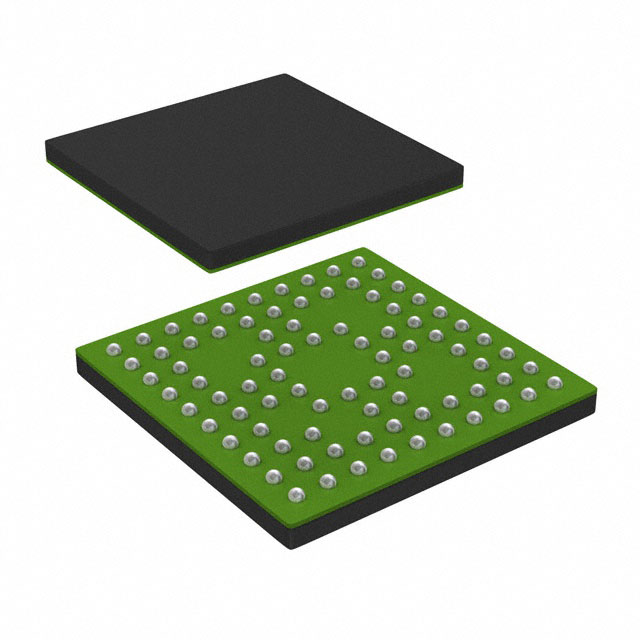
- Part No.:
- CEC1712H-B2-I/SX
- Manufacturer:
- Microchip Technology
- Category:
- Application Specific Microcontrollers
- Package:
- 84-WFBGA
- Datasheet:
-
 CEC1712H-B2-I/SX.pdf
- Description:
- CRYPTO EMBEDDED CTLR FOR SECURE
- Quantity:
- Payment:

- Shipping:

Inventory:153
Please send an inquiry. Send us your inquiry, and we will respond immediately.
Product details
Overview
CEC1712H-B2-I/SX from Microchip Technology is a cryptographic embedded controller featuring an ARM® Cortex-M4 core running up to 48 MHz, 256 KB SRAM (224 KB code + 32 KB data), dual-voltage I/O (1.8 V/3.3 V), and hardware-accelerated crypto engines for AES-256, ECDSA P-384, SHA-384, RSA up to 4096-bit, and TRNG. It serves as a secure, low-power EC in PC platform power management and firmware integrity enforcement.
For engineers reviewing the CEC1712H-B2-I/SX datasheet, CEC1712H-B2-I/SX pinout, CEC1712H-B2-I/SX application, or CEC1712H-B2-I/SX equivalent, key selection criteria include secure boot with immutable ROM, battery-backed RTC and hibernation timers, 5 SMBus/I²C controllers with full crossbar, 6 PWM outputs, and 84-pin WFBGA packaging compatible with modern laptop and desktop motherboard layouts.
Technical Context
The CEC1712H-B2-I/SX implements a tightly coupled ARM Cortex-M4 subsystem with dedicated ITCM and DTCM memory regions, integrated EC interrupt aggregator supporting 5 ACPI power states, and hierarchical sleep architecture including Light/Heavy Sleep modes with sub-10 µA standby current. Its clock system combines a 48 MHz internal PLL with dual 32 kHz sources (internal oscillator + external crystal).
Security is enforced via Boot ROM–based secure loader that validates SPI Flash images using ECDSA P-384 signatures and SHA-384 hashes before execution, while hardware crypto engines offload symmetric (AES), asymmetric (RSA/ECC), and hashing (SHA-1 to SHA-512) operations - all accessible through runtime APIs in ROM. OTP (288 bytes) supports lockable key storage with 32-byte granularity.
Key Specifications
| Parameter | Value and Actual Design Meaning |
|---|---|
| CPU Core | ARM Cortex-M4 @ up to 48 MHz; fixed-point, single 4 GB address space with NVIC and JTAG/SWD debug support. |
| Memory | 256 KB SRAM (224 KB code-optimized + 32 KB data-optimized), 64 B battery-backed SRAM, 288 B OTP, ROM with boot loader and crypto APIs. |
| Power Supply | Separate 3.3 V and 1.8 V I/O rails; operates from -40°C to +85°C; supports ACPI S0–S5 states and chip-level Light/Heavy Sleep. |
| Crypto Acceleration | AES-128/256, ECDSA/EC_KCDSA, RSA 1024–4096 bit, ECC prime/binary field up to 571 bit, SHA-1/256/384/512, TRNG with 1 kbit FIFO. |
| Peripherals | 5 SMBus/I²C controllers (10 configurable ports), 3 UARTs (NS16C550A-compatible), 6 PWM, 2 TACH, 5-channel 10/12-bit ADC, RTC, hibernation & week timers, breathing LED interface. |
| Package | 84-pin WFBGA (5.0 × 5.0 mm, 0.5 mm pitch); 68 GPIOs including 8 over-voltage tolerant pins and 1 battery-powered GPIO (BGPO). |
Pinout & Package
CEC1712H-B2-I/SX is housed in an 84-pin WFBGA package (5.0 × 5.0 mm, 0.5 mm pitch) with dual I/O voltage domains (1.8 V / 3.3 V), full glitch and under-voltage protection on all GPIOs, and 8 over-voltage tolerant pads rated for 3.63 V (1.8 V rail) or 5.5 V (3.3 V rail).
| Pin/Terminal | Circuit Role | Design Meaning |
|---|---|---|
| nRESET_IN | Active-low reset input | Asynchronous system reset assertion; requires external pull-up; triggers cold boot sequence via Boot ROM. |
| VCC_PWRGD | Power-good status input | GPIO057 used to monitor main power rail stability; enables EC wake from sleep upon valid VCC presence. |
| PWROK | Power-ok output | GPIO106 driven high after successful EC initialization; signals host platform readiness to release CPU reset. |
| ICT0_TACH0 / ICT1_TACH1 | Fan tachometer inputs | GPIO050/GPIO051 configured as edge-triggered capture inputs; support 16-bit resolution fan speed measurement. |
| LED0 / LED1 | Breathing LED outputs | GPIO156/GPIO157 drive 5 V–tolerant LEDs with programmable rise/fall waveforms and operation in all EC sleep states. |
| XTAL1 / XTAL2 | 32.768 kHz crystal interface | Differential crystal connection for RTC and hibernation timer; supports external single-ended 32 kHz clock as alternative source. |
| VCI_IN0# / VCI_IN3# | VBAT-powered control inputs | Two active-low inputs (GPIO163/GPIO000) detect system power presence to gate RTC wake events during hibernation. |
| VBAT | Battery backup supply | Connects to coin cell or backup rail; powers RTC, 64 B SRAM, hibernation/week timers, and VCI logic during main power loss. |
Key Features
| Feature | Design Value |
|---|---|
| Secure Boot with Immutable Code | Hardware root of trust enforces ECDSA P-384 signature verification and SHA-384 hash authentication of SPI Flash firmware before loading - prevents unauthorized code execution. |
| Dual-Voltage I/O Banks | Two independent 1.8 V / 3.3 V configurable IO regions enable direct interfacing with both legacy platforms and modern PCHs without level shifters. |
| Full-Crossbar I²C/SMBus | 10 configurable I²C ports routed via crossbar switch to 5 controllers - allows dynamic reassignment of peripherals without PCB changes. |
| Battery-Powered Real-Time Subsystems | RTC, hibernation timers, week timer, and VCI operate from VBAT alone - enabling precise wake scheduling and power-state coordination across full system suspend cycles. |
| Hardware Crypto Offload | Dedicated AES, public-key, and hash engines reduce CPU load by >90% for TLS handshake, firmware signing, and secure boot - critical for deterministic real-time EC response. |
Applications
| Laptop Platform Power Management | Desktop Motherboard EC |
|---|---|
Use Scenario: Managing thermal throttling, fan control, keyboard backlighting, and lid-open detection in thin-and-light notebooks. IC Role / Device Role / Timing Role: Primary embedded controller coordinating ACPI S3/S4 transitions, interpreting PCH-side SMBus commands, and driving PWM-controlled fans via ICT inputs. Use Value: Enables sub-10 µA deep-sleep current and deterministic wake latency (<500 µs) using hibernation timers and VCI-gated RTC alarms. | Use Scenario: Providing secure boot validation, power sequencing, and out-of-band management interfaces on ATX motherboards. IC Role / Device Role / Timing Role: Cryptographic EC enforcing firmware image authenticity prior to CPU initialization; synchronizes PWROK with VCC_PWRGD and RTC-based power-on scheduling. Use Value: Delivers hardware-enforced chain-of-trust with AES-256 encrypted SPI Flash support and roll-back protection against malicious firmware updates. |
| Industrial Control Panel EC | Embedded Thin Client Security Module |
Use Scenario: Serving as trusted execution environment for HMI power control, sensor monitoring (ADC), and LED status indication in factory HMIs. IC Role / Device Role / Timing Role: Standalone secure controller handling button debouncing, breathing LED animation, thermistor-based temperature sensing, and watchdog supervision. Use Value: Integrates 5-channel ADC, 6 PWMs, and 2 TACH inputs with battery-backed RTC - eliminating need for discrete analog and timing ICs. | Use Scenario: Acting as isolated security co-processor for credential storage, secure key derivation, and TLS acceleration in zero-trust endpoint devices. IC Role / Device Role / Timing Role: Dedicated cryptographic engine performing ECDSA signing, RSA decryption, and SHA-384 hashing - decoupled from main application processor. Use Value: Provides FIPS-aligned crypto acceleration with lockable OTP for private keys and DICE-compliant device identity attestation. |
Equivalent & Alternatives
The following parts are listed as comparable options for similar cryptographic embedded controller applications.
| Alternative Part | Technical Difference | Application Difference | Selection Advice |
|---|---|---|---|
| CEC1702H-B2-I/SX | Same ARM Cortex-M4 core and crypto engines, but 64 KB SRAM (vs. 256 KB) and no hibernation timer; 64-pin WFBGA. | Limited peripheral count and memory - suitable only for cost-sensitive, non-RTC-critical EC roles. | Select when board space and BOM cost outweigh need for advanced power-state timers and large firmware footprint. |
| STM32L562VE | ARM Cortex-M33 with TrustZone, 640 KB Flash/256 KB RAM, AES/SHA/RSA accelerators, but no dedicated EC peripherals (SMBus host, PWROK, VCI). | General-purpose secure MCU requiring external logic for ACPI signaling and platform power coordination. | Select when full RTOS deployment, USB, or display interfaces are required - not for drop-in EC replacement. |
Compared with CEC1712H-B2-I/SX, the CEC1702H-B2-I/SX reduces memory and timer capability for lower cost, while the STM32L562VE trades EC-specific hardware (PWROK, VCI, SMBus host) for broader MCU flexibility - neither offers pin-compatible or functional drop-in replacement.
Availability
CEC1712H-B2-I/SX is available at Aetrix Electronics and suitable for laptop platform power management, desktop motherboard EC integration, and industrial HMI control requiring stable component supply, long-term lifecycle assurance, and traceable sourcing.
Supply support for CEC1712H-B2-I/SX includes scheduled delivery planning, volume procurement assistance, BOM continuity management, traceable sourcing, and lifecycle availability coordination for OEM customers, industrial embedded developers, connected-device designers, and electronics production programs.
Manufacturer
Microchip Technology Inc. is a leading provider of microcontrollers, analog components, and security solutions, headquartered in Chandler, Arizona, with global design and manufacturing operations.
The CEC1712H-B2-I/SX belongs to Microchip's Cryptographic Embedded Controller product line, engineered specifically for secure, low-power platform management in PC-class and industrial systems requiring hardware-rooted trust and ACPI-compliant power orchestration.
FAQ
What is the primary function of the CEC1712H-B2-I/SX in a computing platform?
The CEC1712H-B2-I/SX functions as a cryptographic embedded controller responsible for secure boot validation, ACPI power-state coordination (S0–S5), platform power sequencing, and real-time peripheral management. Its ARM Cortex-M4 core executes firmware that authenticates SPI Flash images using ECDSA P-384 and SHA-384 before loading, ensuring only signed code runs - making CEC1712H-B2-I/SX essential for establishing hardware-rooted trust in laptops and desktops.
Does the CEC1712H-B2-I/SX support both 1.8 V and 3.3 V I/O interfaces simultaneously?
Yes, the CEC1712H-B2-I/SX features two separate, configurable I/O voltage domains - one for 1.8 V and another for 3.3 V operation - allowing simultaneous interfacing with modern low-voltage PCHs and legacy 3.3 V peripherals. Each domain supports programmable drive strength (2 mA to 12 mA), pull-up/down control, and glitch/under-voltage protection, and the CEC1712H-B2-I/SX maintains full functionality across both rails without external level shifters.
How does the secure boot process work on the CEC1712H-B2-I/SX?
Upon reset, the CEC1712H-B2-I/SX executes Boot ROM code that loads and verifies the primary firmware image from external SPI Flash. Verification uses hardware-accelerated ECDSA P-384 signatures and SHA-384 hashes stored in OTP or external storage. If validation passes, the image is loaded into SRAM and executed; if it fails, the CEC1712H-B2-I/SX attempts fallback image loading or halts. AES-256 encryption of SPI Flash contents is also supported, and key revocation and roll-back protection are enforced - all within the immutable Boot ROM of CEC1712H-B2-I/SX.
Can the CEC1712H-B2-I/SX operate independently during system hibernation?
Yes, the CEC1712H-B2-I/SX maintains full functionality during hibernation using its VBAT supply. The RTC, two hibernation timers, week timer, VCI inputs, and battery-backed 64 B SRAM remain active - enabling precise wake scheduling (down to 0.5 ms resolution) and power-event detection even when main VTR rails are off. This autonomous operation is central to the CEC1712H-B2-I/SX role in managing low-power states without host CPU involvement.
What debugging interfaces are available on the CEC1712H-B2-I/SX?
The CEC1712H-B2-I/SX provides three standardized debug interfaces: a 4-pin JTAG port for boundary scan and full-chip debug, a 2-pin Serial Wire Debug (SWD) interface for streamlined firmware development, and a Trace FIFO Debug Port (TFDP) supporting real-time instruction and data trace. All interfaces are accessible via dedicated pins (e.g., JTAG_TDI/TDO/TMS/TCK, SWDIO/SWCLK, TFDP_CLK/DATA), and JTAG is disabled by default - enhancing security unless explicitly enabled via OTP configuration in CEC1712H-B2-I/SX.
CEC1712H-B2-I/SX Specifications
- Product attributes
- Attribute value
- Manufacturer:
- Microchip Technology
- Series:
- CryptoController™
- Package/Case:
- 84-WFBGA
- Packaging:
- Tray
- Product Status:
- Active
- Programmable:
- Not Verified
- Applications:
- Cryptography
- Core Processor:
- ARM® Cortex®-M4F
- Program Memory Type:
- -
- Controller Series:
- -
- RAM Size:
- 256K x 8
- Interface:
- I2C, SPI, UART
- Number of I/O:
- 68
- Voltage - Supply:
- 1.71V ~ 3.465V
- Operating Temperature:
- -40°C ~ 85°C (TA)
- Grade:
- -
- Qualification:
- -
- Mounting Type:
- Surface Mount
- Supplier Device Package:
- 84-WFBGA (7x7)
CEC1712H-B2-I/SX FAQ
1.How can I place an order for CEC1712H-B2-I/SX through Aetrix?
Please submit a Request for Quotation (RFQ) for CEC1712H-B2-I/SX on Aetrix. Our sales agent will provide a competitive quotation and guide you through the order confirmation once you accept the terms.
2.Are the price and stock information for CEC1712H-B2-I/SX reliable?
The price and inventory of CEC1712H-B2-I/SX are updated periodically and may fluctuate due to market conditions. Stock and pricing data are typically refreshed every 24 hours. Quotation validity for CEC1712H-B2-I/SX is usually 5 days.
3.What payment methods are accepted for CEC1712H-B2-I/SX?
We accept Wire Transfer, PayPal, Credit Card, Western Union, MoneyGram, and Escrow for CEC1712H-B2-I/SX transactions.
Note: Certain payment methods may incur a processing fee.
4.How is shipping managed for CEC1712H-B2-I/SX?
CEC1712H-B2-I/SX orders can be shipped via leading logistics carriers, including DHL, UPS, FedEx, TNT, or Registered Mail.
Once your CEC1712H-B2-I/SX order is processed, you will receive an email with the shipment details and tracking number.
Note: Tracking information may take up to 24 hours to appear. Express delivery typically takes 3–5 business days.
5.How can I obtain technical support or documentation for CEC1712H-B2-I/SX?
For technical support, including CEC1712H-B2-I/SX datasheets, pinout diagrams, or application guidance, please contact our engineering support team. They can provide detailed documentation and assistance for your CEC1712H-B2-I/SX requirements.
6.How does Aetrix verify that CEC1712H-B2-I/SX is sourced from the original manufacturer or authorized distributors?
All CEC1712H-B2-I/SX products on Aetrix are procured from qualified distributors and authorized channels. Our dedicated quality assurance team conducts strict verification, including traceability checks and, if necessary, third-party testing. This ensures that CEC1712H-B2-I/SX meets industry standards.
7.What is the process for return or replacement of CEC1712H-B2-I/SX?
All CEC1712H-B2-I/SX units undergo pre-shipment inspection (PSI). If there is an issue with CEC1712H-B2-I/SX, returns or replacements are accepted under the following conditions:
1.Quantity discrepancies, incorrect items, or visible external defects (such as breakage or corrosion), acknowledged by Aetrix.
2.The issue is reported within 90 days of delivery.
3.The CEC1712H-B2-I/SX part is unused and in its original packaging.
Return procedure for CEC1712H-B2-I/SX:
1.Submit a request within 90 days.
2.Obtain a Return Material Authorization (RMA) from Aetrix.
CEC1712H-B2-I/SX Tags

-
CYPD3175-24LQXQ
Infineon Technologies

-
SLB9672VU20FW1523XTMA1
Infineon Technologies

-
SLB9670VQ20FW785XTMA1
Infineon Technologies
-
SLB9672XU20FW1523XTMA1
Infineon Technologies
-
SLB9673XU20FW2613XTMA1
Infineon Technologies

-
CYPD3125-40LQXIT
Infineon Technologies

-
AT97SC3204-U2A1A-20
Microchip Technology
-
AT97SC3204-U2A1A-10
Microchip Technology
-
SLM9670AQ20FW1311XTMA1
Infineon Technologies
-
SLB9672XU20FW1613XTMA1
Infineon Technologies
-
SLB9672AU20FW1613XTMA1
Infineon Technologies
-
SLB9673AU20FW2613XTMA1
Infineon Technologies
Tech Hub

TTL and CMOS logic families differ in thresholds, loading, output drive, power and timing. This engineering guide compares 74HC and 74HCT, calculates noise margins and checks 3.3 V/5 V compatibility.

A practical engineering guide to 3.3V and 5V logic compatibility, input thresholds, resistor dividers, translator ICs, MOSFET level shifting, I2C pull-ups, timing limits and power-sequencing risks.

The 74HC595 uses push-pull logic outputs, while the TPIC6B595 uses 50 V open-drain DMOS sinks for higher-power loads. This guide compares timing, current limits, 3.3 V interfacing, load wiring, thermal…

The 74HC595 converts serial data into eight stable parallel outputs. This guide covers pin functions, shift and storage timing, OE and MR behavior, drive-current limits, cascading, voltage compatibilit…

A technical comparison of level-sensitive latches and edge-triggered flip-flops, covering timing windows, setup and hold limits, master–slave operation, time borrowing, race-through, HDL inference and…

A D latch stores one bit while Enable controls when data can pass. This reference covers gate-level operation, truth tables, transparency, setup and hold timing, LE versus OE, common ICs and practical …

An SR latch stores one bit through cross-coupled feedback. This engineering reference covers NOR and NAND implementations, truth tables, forbidden-state recovery, gated operation, switch debouncing, fa…

Latch circuits retain one bit through feedback. This technical reference covers SR and D latches, truth tables, transparency, timing limits, latch-versus-flip-flop behavior, applications and common log…

An engineering guide to LED driver operation, constant-current and constant-voltage outputs, linear and switching topologies, dimming, IC selection, calculations, replacement compatibility, and fault c…

Operational amplifier guide covering op amp basics, feedback, ideal vs real op amps, common configurations, buffer circuits, offset, bias current, gain-bandwidth, slew rate, rail-to-rail limits and sel…


