
 My Inquiry
 My Account


Microchip Technology CW01K6-G
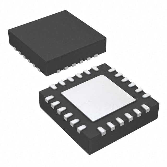
- Part No.:
- CW01K6-G
- Manufacturer:
- Microchip Technology
- Category:
- Power Management - Specialized
- Package:
- 24-VFQFN Exposed Pad
- Datasheet:
-
 CW01K6-G.pdf
- Description:
- IC TRANSMITTER 4CH 24QFN
- Quantity:
- Payment:

- Shipping:

Inventory:4,221
Please send an inquiry. Send us your inquiry, and we will respond immediately.
Product details
Overview
CW01K6-G from Microchip Technology is a 4-channel low-phase-noise continuous wave (CW) transmitter IC designed for high-precision ultrasonic excitation. It integrates four independent N-channel gate drivers with 100 V open-drain outputs, a high-speed D flip-flop per channel synchronized to up to 200 MHz clock input, and dual undervoltage lockout (UVLO) on VDD and VLL. It is used in diagnostic medical ultrasound transmitters requiring precise timing alignment and minimal jitter across channels.
For engineers reviewing the CW01K6-G datasheet, CW01K6-G pinout, CW01K6-G application, or CW01K6-G equivalent, key selection considerations include its 100 V output capability, 4.7 Ω typical on-resistance, –171 dBc/Hz phase noise at 1 kHz offset (80 MHz CLK), 5.1 ns CLK-to-HVOUT delay matching, and dedicated per-channel gate drive supply pins (VD1–VD4) for crosstalk suppression.
Technical Context
The CW01K6-G implements four independent high-speed D flip-flops, each clocked on the rising edge of a common CLK signal, enabling synchronous alignment of DIN1–DIN4 inputs to a high-frequency reference. Each channel features isolated gate drive voltage supplies (VD1–VD4) and power grounds (PGND1–PGND4) to minimize supply-induced jitter and inter-channel coupling.
It incorporates dual UVLO circuitry-separate thresholds at 1.5 V for VLL and 4.0 V for VDD-to prevent spurious output activation during power ramp-up. The HVOUT outputs operate as open-drain N-channel switches capable of sinking up to 0.8 A saturation current with 4.7 Ω typical on-resistance, driven by logic-level inputs referenced to VLL (1.65–5.5 V range).
Key Specifications
| Parameter | Value and Actual Design Meaning |
|---|---|
| Output Channels | 4 independent high-voltage switch channels with individual VDx/PGNDx routing |
| Max Clock Frequency | 200 MHz - enables precise sub-ns timing control for phased-array ultrasound beamforming |
| HVOUT Voltage Rating | 100 V - supports high-voltage PZT transducer excitation without external level-shifting |
| Phase Noise | –171 dBc/Hz @ 1 kHz offset (80 MHz CLK) - critical for low-jitter continuous-wave Doppler signal generation |
| CLK-to-HVOUT Delay Matching | ±0.5 ns (ΔtdLH/ΔtdHL) - ensures tight inter-channel timing alignment for coherent multi-element driving |
| On-resistance (RON) | 4.7 Ω typical - minimizes conduction loss and self-heating during high-current PZT pulsing |
| UVLO Thresholds | VLL: 1.5 V, VDD: 4.0 V - prevents false triggering during brown-out or incomplete power sequencing |
Pinout & Package
24-lead QFN package (4.0 mm × 5.0 mm, 0.5 mm pitch, 1.0 mm max height), RoHS-compliant, lead-free matte tin finish. Exposed thermal pad (center) must be externally shorted to all PGND and VSS pins for thermal and electrical integrity.
| Pin/Terminal | Circuit Role | Design Meaning |
|---|---|---|
| DIN1–DIN4 | Per-channel D flip-flop data input | Logic-high input clocks through to enable corresponding HVOUT; referenced to VLL |
| CLK | Global synchronous clock input | Rising-edge-triggered; controls all four D flip-flops simultaneously for time-aligned switching |
| OE | Global output enable | Active-low; disables all HVOUT outputs when logic low, independent of DIN states |
| VD1–VD4 | Per-channel gate drive supply | Provides dedicated 4.5–5.5 V bias for each N-channel driver; decoupling required to suppress jitter |
| HVOUT1–HVOUT4 | High-voltage open-drain outputs | Drain terminals capable of 100 V swing and 0.8 A saturation; connect to PZT transducer elements |
| PGND1–PGND4 | Per-channel power ground | Isolated return paths for HVOUT currents; must be shorted externally to VSS to avoid ground bounce |
| VDD / VLL / VSS | Level translator / logic supply / system ground | VDD (4.5–5.5 V) powers internal logic translation; VLL (1.65–5.5 V) sets logic threshold; VSS is common reference |
Key Features
| Feature | Design Value |
|---|---|
| Per-channel gate drive supply (VDx) | Enables independent decoupling per channel to reduce crosstalk and output jitter below 1 ps RMS |
| Low phase noise architecture | –171 dBc/Hz at 1 kHz offset supports high-resolution Doppler spectral analysis in medical imaging |
| High-speed D flip-flop synchronization | 200 MHz clock tolerance allows precise timing alignment of four output pulses within ±0.5 ns skew |
| 100 V open-drain N-channel outputs | Eliminates need for external high-voltage level shifters when driving 50–100 V PZT transducers |
| Dual UVLO protection | Independent 1.5 V (VLL) and 4.0 V (VDD) trip points prevent erratic switching during partial power-up sequences |
Applications
| Diagnostic Medical Ultrasound | Fluid Flow Measurement |
|---|---|
Use Scenario: Driving piezoelectric transducer arrays in portable and cart-based ultrasound systems for B-mode and Doppler imaging. IC Role / Device Role / Timing Role: 4-channel CW transmitter providing synchronized, low-jitter high-voltage pulses to excite PZT elements in phased-array configurations. Use Value: –171 dBc/Hz phase noise and ±0.5 ns inter-channel delay matching enable clean Doppler signal acquisition and high-contrast blood flow visualization. | Use Scenario: Exciting ultrasonic transducers in industrial flow meters measuring liquid or gas velocity via time-of-flight or Doppler shift. IC Role / Device Role / Timing Role: High-voltage pulse generator delivering precisely timed bursts to transmit/receive transducers operating at 2–5 MHz. Use Value: 100 V output rating and 4.7 Ω RON support efficient energy transfer into high-impedance transducers, improving SNR and measurement accuracy. |
| Non-Destructive Testing (NDT) | Acoustic Imaging Systems |
Use Scenario: Pulse-echo inspection of composite materials, welds, or castings using broadband ultrasonic transducers. IC Role / Device Role / Timing Role: Low-phase-noise CW source generating stable excitation signals for high-resolution defect detection. Use Value: Dedicated VDx/PGNDx routing minimizes channel-to-channel crosstalk, preserving signal fidelity in multi-element array receivers. | Use Scenario: Driving transducer arrays in underwater sonar or biomedical photoacoustic imaging systems requiring coherent multi-channel excitation. IC Role / Device Role / Timing Role: Synchronized 4-channel transmitter enabling beam steering and focusing via controlled phase delays. Use Value: 200 MHz clock interface and sub-ns delay matching allow digital synthesis of complex waveform envelopes for adaptive beamforming. |
Equivalent & Alternatives
The following parts are listed as comparable options for similar high-voltage ultrasonic transmitter applications.
| Alternative Part | Technical Difference | Application Difference | Selection Advice |
|---|---|---|---|
| Supertex HV809 | 8-channel, 120 V rated, no integrated D flip-flop; requires external timing logic | Lacks on-chip clock synchronization; higher channel count but greater board complexity | Choose when >4 channels needed and external FPGA/CPLD timing control is available |
| Texas Instruments DRV2700 | Integrated boost converter + H-bridge driver; 100 V, but single-channel and analog-input only | Designed for resonant piezo driving with closed-loop amplitude control, not CW burst timing | Prefer for amplitude-stabilized resonant excitation rather than multi-channel synchronous pulsing |
Compared with HV809 and DRV2700, the CW01K6-G uniquely combines 4-channel integration, on-die D flip-flop synchronization, per-channel gate supply isolation, and ultra-low phase noise-making it optimal for compact, low-jitter, multi-element CW ultrasound transmitters where timing coherence and jitter suppression are design-critical.
Availability
CW01K6-G is available at Aetrix Electronics and suitable for diagnostic medical ultrasound, fluid flow measurement, and non-destructive testing applications requiring stable component supply, long-term lifecycle support, and traceable sourcing.
Supply support for CW01K6-G includes scheduled delivery planning, volume procurement assistance, BOM continuity management, traceable sourcing, and lifecycle availability coordination for OEM customers, industrial embedded developers, connected-device designers, and electronics production programs.
Manufacturer
Microchip Technology is a U.S.-based semiconductor company specializing in microcontrollers, analog devices, FPGAs, and timing solutions, with ISO/TS-16949-certified manufacturing.
The CW01 product line was developed specifically for high-precision, low-jitter continuous-wave ultrasonic transmission in medical and industrial sensing, emphasizing channel isolation, timing fidelity, and high-voltage robustness.
FAQ
What is the maximum allowable voltage on the HVOUT pins of the CW01K6-G?
The CW01K6-G specifies an absolute maximum HVOUT drain voltage of –0.5 V to +120 V. Its operational high-voltage output rating is 100 V, verified under DC and pulsed conditions per the datasheet's Electrical Characteristics table. Exceeding 100 V during normal operation risks reliability degradation; the 120 V limit is a stress rating only and not intended for functional use. Always observe the 100 V design limit in CW01K6-G applications.
Does the CW01K6-G require external level-shifting circuitry to drive PZT transducers?
No, the CW01K6-G does not require external level-shifting circuitry to drive typical PZT transducers. Its 100 V open-drain N-channel outputs and integrated level translator (VDD/VLL architecture) enable direct connection to transducers operating up to 100 V. The device accepts logic-level DIN inputs referenced to VLL (1.65–5.5 V), eliminating the need for discrete MOSFET translators or gate driver ICs in most CW ultrasound designs using the CW01K6-G.
How is inter-channel timing skew minimized in the CW01K6-G?
The CW01K6-G minimizes inter-channel timing skew through three design features: (1) a single global CLK input synchronizing all four internal D flip-flops, (2) matched internal propagation paths yielding ±0.5 ns delay matching (ΔtdLH/ΔtdHL), and (3) physically isolated per-channel gate drive supplies (VD1–VD4) and power grounds (PGND1–PGND4) to suppress supply-induced jitter. These ensure sub-nanosecond coherence essential for phased-array beamforming in the CW01K6-G.
Can the CW01K6-G operate with different supply voltages on VD1–VD4?
Yes, the CW01K6-G allows independent setting of VD1–VD4 supply voltages within the 4.5–5.5 V range, though the datasheet recommends maintaining them at the same potential as VDD for optimal performance. This flexibility enables fine-tuning of rise/fall times and drive strength per channel-for example, adjusting VD1 for a higher-power transducer while keeping VD2–VD4 at nominal 5 V. All VDx pins must remain within absolute maximum ratings (–0.5 V to +6 V) to avoid damage to the CW01K6-G.
What thermal management is required for the CW01K6-G in continuous operation?
The CW01K6-G has a junction-to-ambient thermal resistance (θJA) of 26.9°C/W when mounted on a 4-layer 3"×4" PCB. At full load (all four channels active, fCLK = 200 MHz), total power dissipation reaches ~3 W. To maintain TJ ≤ 125°C at TA = 85°C, ≥2.5 cm² of 2-oz copper connected to the exposed thermal pad is recommended. The center pad must be soldered and shorted to all PGND/VSS pins; insufficient thermal relief will cause thermal shutdown or accelerated parametric drift in the CW01K6-G.
CW01K6-G Specifications
- Product attributes
- Attribute value
- Manufacturer:
- Microchip Technology
- Series:
- -
- Package/Case:
- 24-VFQFN Exposed Pad
- Packaging:
- Tape & Reel (TR)
- Product Status:
- Active
- Applications:
- Continuous Wave Transmitter
- Current - Supply:
- 23.5mA
- Voltage - Supply:
- 4.5V ~ 5.5V
- Operating Temperature:
- -40°C ~ 125°C
- Grade:
- -
- Qualification:
- -
- Mounting Type:
- Surface Mount
- Supplier Device Package:
- 24-QFN (5x4)
CW01K6-G FAQ
1.How can I place an order for CW01K6-G through Aetrix?
Please submit a Request for Quotation (RFQ) for CW01K6-G on Aetrix. Our sales agent will provide a competitive quotation and guide you through the order confirmation once you accept the terms.
2.Are the price and stock information for CW01K6-G reliable?
The price and inventory of CW01K6-G are updated periodically and may fluctuate due to market conditions. Stock and pricing data are typically refreshed every 24 hours. Quotation validity for CW01K6-G is usually 5 days.
3.What payment methods are accepted for CW01K6-G?
We accept Wire Transfer, PayPal, Credit Card, Western Union, MoneyGram, and Escrow for CW01K6-G transactions.
Note: Certain payment methods may incur a processing fee.
4.How is shipping managed for CW01K6-G?
CW01K6-G orders can be shipped via leading logistics carriers, including DHL, UPS, FedEx, TNT, or Registered Mail.
Once your CW01K6-G order is processed, you will receive an email with the shipment details and tracking number.
Note: Tracking information may take up to 24 hours to appear. Express delivery typically takes 3–5 business days.
5.How can I obtain technical support or documentation for CW01K6-G?
For technical support, including CW01K6-G datasheets, pinout diagrams, or application guidance, please contact our engineering support team. They can provide detailed documentation and assistance for your CW01K6-G requirements.
6.How does Aetrix verify that CW01K6-G is sourced from the original manufacturer or authorized distributors?
All CW01K6-G products on Aetrix are procured from qualified distributors and authorized channels. Our dedicated quality assurance team conducts strict verification, including traceability checks and, if necessary, third-party testing. This ensures that CW01K6-G meets industry standards.
7.What is the process for return or replacement of CW01K6-G?
All CW01K6-G units undergo pre-shipment inspection (PSI). If there is an issue with CW01K6-G, returns or replacements are accepted under the following conditions:
1.Quantity discrepancies, incorrect items, or visible external defects (such as breakage or corrosion), acknowledged by Aetrix.
2.The issue is reported within 90 days of delivery.
3.The CW01K6-G part is unused and in its original packaging.
Return procedure for CW01K6-G:
1.Submit a request within 90 days.
2.Obtain a Return Material Authorization (RMA) from Aetrix.
CW01K6-G Tags

-
TPS2511DGNR
Texas Instruments

-
UTC2000/MG
Microchip Technology

-
TUSB320HAIRWBR
Texas Instruments

-
TPS61252DSGR
Texas Instruments

-
PI5USB30216CXUAEX
Diodes Incorporated

-
SN6501DBVR
Texas Instruments

-
CYPD3177-24LQXQT
Infineon Technologies
-
SN6501QDBVRQ1
Texas Instruments

-
STUSB1600AQTR
STMicroelectronics

-
SN6505BDBVR
Texas Instruments
-
SN6501DBVT
Texas Instruments

-
TPS65150PWPR
Texas Instruments
Tech Hub

TTL and CMOS logic families differ in thresholds, loading, output drive, power and timing. This engineering guide compares 74HC and 74HCT, calculates noise margins and checks 3.3 V/5 V compatibility.

A practical engineering guide to 3.3V and 5V logic compatibility, input thresholds, resistor dividers, translator ICs, MOSFET level shifting, I2C pull-ups, timing limits and power-sequencing risks.

The 74HC595 uses push-pull logic outputs, while the TPIC6B595 uses 50 V open-drain DMOS sinks for higher-power loads. This guide compares timing, current limits, 3.3 V interfacing, load wiring, thermal…

The 74HC595 converts serial data into eight stable parallel outputs. This guide covers pin functions, shift and storage timing, OE and MR behavior, drive-current limits, cascading, voltage compatibilit…

A technical comparison of level-sensitive latches and edge-triggered flip-flops, covering timing windows, setup and hold limits, master–slave operation, time borrowing, race-through, HDL inference and…

A D latch stores one bit while Enable controls when data can pass. This reference covers gate-level operation, truth tables, transparency, setup and hold timing, LE versus OE, common ICs and practical …

An SR latch stores one bit through cross-coupled feedback. This engineering reference covers NOR and NAND implementations, truth tables, forbidden-state recovery, gated operation, switch debouncing, fa…

Latch circuits retain one bit through feedback. This technical reference covers SR and D latches, truth tables, transparency, timing limits, latch-versus-flip-flop behavior, applications and common log…

An engineering guide to LED driver operation, constant-current and constant-voltage outputs, linear and switching topologies, dimming, IC selection, calculations, replacement compatibility, and fault c…

Operational amplifier guide covering op amp basics, feedback, ideal vs real op amps, common configurations, buffer circuits, offset, bias current, gain-bandwidth, slew rate, rail-to-rail limits and sel…


