
 My Inquiry
 My Account


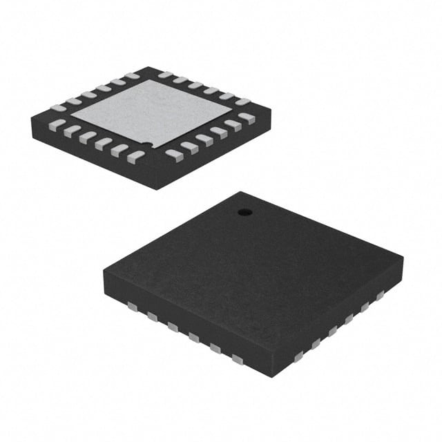
Infineon Technologies CYPD3196-24LDXS
- Part No.:
- CYPD3196-24LDXS
- Manufacturer:
- Infineon Technologies
- Category:
- Application Specific Microcontrollers
- Package:
- 24-UFQFN Exposed Pad
- Datasheet:
-
 CYPD3196-24LDXS.pdf
- Description:
- CCG3PA
- Quantity:
- Payment:

- Shipping:

Inventory:870
Please send an inquiry. Send us your inquiry, and we will respond immediately.
Product details
Overview
CYPD3196-24LDXS from Cypress Semiconductor is a single-chip, AEC-Q100 qualified USB Type-C port controller with integrated Arm® Cortex®-M0 MCU (64 KB Flash, 8 KB SRAM), full USB PD 3.0 v1.1 support including Programmable Power Supply mode, dual-port capability (one Type-C + one Type-A), and automotive-grade VBUS regulation (3.0–24.5 V input, ±8-kV contact ESD). It targets rear-seat automotive chargers requiring robust fault protection, legacy charging detection (QC 4.0, Apple 2.4A, AFC, BC 1.2), and system-level thermal/power management.
For engineers reviewing the CYPD3196-24LDXS datasheet, CYPD3196-24LDXS pinout, CYPD3196-24LDXS application, or CYPD3196-24LDXS equivalent, key selection criteria include its integrated shunt-based VBUS regulation, dual 8-bit SAR ADCs for temperature/current monitoring, wettable-flank 24-pin QFN package for automotive reflow inspection, and native support for BMC-encoded PD communication over CC lines without external transceivers.
Technical Context
The device implements a dedicated USB-PD physical layer with BMC encoder/decoder, hardware collision avoidance, and configurable RP/RD termination for DFP role enforcement. Its high-voltage regulator supports constant-voltage and constant-current VBUS control via feedback pin (FB) and integrates low-side current sense amplifier (CSA) with 100 mA resolution across 5 mΩ shunt.
Two integrated PFET gate drivers (VBUS_P_CTRL with active pull-up; VBUS_C_CTRL requiring external pull-up) manage power path switching, while four VBUS-short-protected pins (CC1, CC2, P2.2, P2.3) withstand up to 22 VDC for 1000 hours-critical for automotive connector layout where CC pins neighbor VBUS.
Key Specifications
| Parameter | Value and Actual Design Meaning |
|---|---|
| USB-PD Compliance | PD 3.0 v1.1 with Programmable Power Supply (PPS) mode support for adaptive voltage control in fast-charging systems |
| MCU Core | Arm Cortex-M0 @ up to 48 MHz; enables custom firmware for load sharing, power throttling, and charger negotiation logic |
| VBUS Input Range | 3.0 V to 24.5 V (30 V tolerant); allows direct connection to automotive battery rail without external pre-regulator |
| ESD Protection | ±8 kV contact / ±15 kV air-gap per IEC61000-4-2 Level 4C on CC, DP/DM, VBUS_C_MON_DISCHARGE, P2.2/P2.3 |
| ADC Resources | Two 8-bit SAR ADCs with internal bandgap or VDDD reference; supports GPIO/DP/DM analog muxing for temperature and current sensing |
| Charger Detection | Native support for QC 4.0, Apple 2.4A, Samsung AFC, and BC 1.2 via dual DP/DM blocks-no external IC required |
| Package | 24-pin QFN (4 × 4 mm), wettable flank, AEC-Q100 Grade 2 (–40 °C to +105 °C) |
Pinout & Package
Package: 24-pin QFN (4 mm × 4 mm, 0.5 mm pitch), wettable flank, RoHS-compliant, designed for automated optical inspection (AOI) in automotive PCB assembly.
| Pin/Terminal | Circuit Role | Design Meaning |
|---|---|---|
| 1 (P1.0) | GPIO / Fault Indicator | Configurable as OCP/SCP/OVP/UVP fault output; maps any two faults to separate pins or ORs all four to single indicator |
| 2 (P1.1) | GPIO / Fault Indicator | Second dedicated fault reporting pin; enables discrete fault prioritization in safety-critical automotive charging systems |
| 3 (CC1) | Type-C Configuration Channel | VBUS-short-protected BMC data line; handles plug orientation detection, role negotiation, and PD messaging in DFP mode |
| 4 (CC2) | Type-C Configuration Channel | Duplicate CC line with identical VBUS-short protection; ensures redundancy and full Type-C cable compatibility |
| 5 (VBUS_C_MON_DISCHARGE) | VBUS Monitoring & Discharge Control | Analog input for VBUS voltage sensing; drives internal discharge FET to meet USB-PD detach timing (<500 ms ramp-down) |
| 6 (DP0 / GPIO) | Legacy Charger Detection | Direct connection to Type-A port DP line; enables BC 1.2 and proprietary charger signature detection without level shifters |
| 7 (DM0 / GPIO) | Legacy Charger Detection | Paired with DP0 for D+/- handshake; supports Apple, QC 4.0, AFC protocols via firmware-controlled voltage/current profiling |
| 8 (VBUS_IN_DISCHARGE) | Main Power Input | High-voltage input (3.0–24.5 V); powers internal 3.3 V LDO (VDDD) and 1.8 V core regulator (VCCD) for full-system operation |
| 9 (GND) | Power Ground | Primary return path for VBUS_IN_DISCHARGE, analog blocks, and digital logic; requires low-impedance PCB plane connection |
| 10 (VBUS_P_CTRL) | PFET Gate Driver (Provider) | Active pull-up driver for external high-side PFET on VBUS supply path; supports soft-start and current-limited turn-on |
| 11 (VBUS_C_CTRL) | PFET Gate Driver (Consumer) | Open-drain driver requiring external pull-up; controls external PFET on VBUS sink path for consumer-mode discharge control |
| 12 (FB) | VBUS Feedback Input | Analog input for closed-loop VBUS regulation; connects to resistor divider from VBUS to set target voltage per PD contract |
| 13 (CATH/COMP) | Shunt Regulator Compensation | Connects to external compensation network for stability of integrated shunt-based VBUS regulation loop |
| 14 (LSCSA) | Low-Side Current Sense Amp | Outputs amplified voltage proportional to current through external 5 mΩ shunt; enables precise CC mode control in charging |
| 15 (Rs) | Current Sense Resistor Ref | Reference node for LSCSA; ties to shunt resistor ground side to reject common-mode noise in high-noise automotive environments |
| 16 (VCCD) | Core Digital Supply | 1.8 V regulated output powering CPU, flash, SRAM, and digital peripherals; must be decoupled with 1 µF ceramic capacitor |
| 17 (VDDD) | Digital I/O Supply | 3.3 V regulated output powering GPIOs, SCBs, and analog mux; not intended to drive external loads-only local decoupling |
| 18 (P0.0) | OVT GPIO | Overvoltage-tolerant (7 V max) general-purpose I/O; suitable for direct interface with 5 V logic or sensor outputs |
| 19 (P0.1) | OVT GPIO | Second overvoltage-tolerant pin; enables robust communication with external PMICs or status indicators in mixed-voltage systems |
| 20 (P2.2) | VBUS-Short Protected GPIO | Protected I/O pin adjacent to VBUS in connector layout; prevents latch-up during accidental shorts in production handling |
| 21 (P2.3) | VBUS-Short Protected GPIO | Redundant protected I/O; used for auxiliary functions like LED control or thermistor biasing near high-voltage zones |
| 22 (DP1 / GPIO) | Secondary Legacy Charger Port | Supports second Type-A port or alternate DP line for multi-port charger designs with independent charging profiles |
| 23 (DM1 / GPIO) | Secondary Legacy Charger Port | Complements DP1 for dual legacy port support; enables simultaneous QC/AFC detection on separate USB outputs |
| 24 (VSS) | Ground Reference | Dedicated analog/digital ground return; must be connected to main system GND plane with minimal trace inductance |
Key Features
| Feature | Design Value |
|---|---|
| Integrated USB-PD PHY | Full BMC encoder/decoder with hardware collision avoidance eliminates need for external transceiver and reduces BOM count by ≥2 ICs |
| Automotive-Grade VBUS Short Protection | Four dedicated pins (CC1/CC2/P2.2/P2.3) withstand 22 VDC for 1000 hours-enables reliable deployment in cramped automotive connectors |
| Dual Legacy Charging Blocks | Independent DP0/DM0 and DP1/DM1 interfaces support concurrent QC 4.0 + Apple 2.4A negotiation on separate ports without resource contention |
| Programmable VBUS Regulation | Shunt-based FB loop with CATH/COMP pins allows stable CV/CC output across 5–20 V range using only passive components |
| On-Chip Fault Protection Suite | Hardware OVP/OCP/UVP/SCP blocks respond in <1 µs; eliminates reliance on software polling for critical automotive safety thresholds |
| Wettable Flank QFN | 24-pin package enables automated X-ray and AOI verification of solder joint integrity-mandatory for Tier-1 automotive qualification |
Applications
| Rear-Seat Automotive Charger | Infotainment Head Unit Charger |
|---|---|
|
Use Scenario: Dual-output USB charging module mounted behind rear seat armrest, powered directly from 12 V battery rail with thermal derating at 60 °C ambient. IC Role / Device Role / Timing Role: Primary Type-C PD controller managing VBUS negotiation, legacy charger detection, and real-time current limiting across both ports. Use Value: Integrates termination resistors, VBUS regulation, and ESD protection-reducing component count by 11 parts versus discrete solution. |
Use Scenario: Integrated USB charging port in center console infotainment system, supporting simultaneous fast charge for smartphone and tablet with dynamic power allocation. IC Role / Device Role / Timing Role: System-level power manager coordinating PD contract updates, temperature monitoring via ADC, and fault-triggered shutdown within 500 µs. Use Value: Enables firmware-defined power throttling to maintain total output ≤36 W while meeting AEC-Q100 thermal cycling requirements. |
| Rear Seat Entertainment (RSE) Charger | Automotive Docking Station |
|
Use Scenario: Multi-port charging hub embedded in RSE screen housing, delivering 15 W to tablet and 7.5 W to wireless earbuds case under continuous 45 °C cabin temperature. IC Role / Device Role / Timing Role: Dual-role controller acting as DFP for Type-C port and legacy charger for Type-A port, with shared thermal management. Use Value: On-die temperature sensor and dual ADCs allow closed-loop derating without external sensors-cutting BOM cost by $0.32/unit. |
Use Scenario: Vehicle-mounted docking station for fleet tablets, requiring hot-plug resilience, PD contract renegotiation on cable swap, and VBUS discharge compliance. IC Role / Device Role / Timing Role: Robust PD protocol engine with VBUS_C_MON_DISCHARGE-driven discharge FET control ensuring <400 ms ramp-down per USB-IF certification. Use Value: Integrated discharge FETs eliminate need for external MOSFETs and timing RC networks-reducing layout area by 28 mm². |
Equivalent & Alternatives
The following parts are listed as comparable options for similar USB Type-C port controller applications.
| Alternative Part | Technical Difference | Application Difference | Selection Advice |
|---|---|---|---|
| STUSB4500QTR | Lacks integrated MCU, flash, and ADCs; relies on external host processor for PD policy engine and thermal management | Suitable for cost-sensitive non-automotive chargers where firmware customization is unnecessary | Select when BOM simplicity outweighs need for autonomous fault response or field-upgradable charging profiles |
| TPS65987DRLR | Higher integration includes integrated DC/DC converter; no native legacy charger detection blocks for QC/AFC/Apple | Better suited for laptop dock applications requiring 100 W PD delivery but no proprietary charging support | Choose only if system already implements separate legacy charging IC and requires higher PD power delivery than CYPD3196's 60 W limit |
Compared with STUSB4500QTR and TPS65987DRLR, CYPD3196-24LDXS uniquely combines automotive-grade robustness, on-chip firmware programmability, and native multi-protocol legacy charging-making it the only option for AEC-Q100-compliant single-chip automotive chargers needing QC 4.0 + PD 3.0 coexistence.
Availability
CYPD3196-24LDXS is available at Aetrix Electronics and suitable for rear-seat automotive chargers, infotainment head unit power supplies, and rear-seat entertainment systems requiring stable component supply, AEC-Q100 qualification, and long-term lifecycle support.
Supply support for CYPD3196-24LDXS includes scheduled delivery planning, volume procurement assistance, BOM continuity management, traceable sourcing, and lifecycle availability coordination for OEM customers, industrial embedded developers, connected-device designers, and electronics production programs.
Manufacturer
Cypress Semiconductor (now part of Infineon Technologies) is a fabless semiconductor company specializing in programmable system-on-chip solutions for automotive, industrial, and consumer electronics.
CYPD319X is part of Cypress' EZ-PD™ portfolio-designed specifically for automotive USB-C charging applications requiring AEC-Q100 qualification, integrated fault protection, and firmware-customizable power management.
FAQ
What is the maximum USB PD power delivery capability supported by CYPD3196-24LDXS?
CYPD3196-24LDXS supports USB PD 3.0 v1.1 up to 60 W (20 V @ 3 A) with Programmable Power Supply mode. Its integrated VBUS regulation loop and current sense amplifier enable precise constant-current control during PPS negotiation, but hardware current limits and thermal design constrain sustained output to 60 W in automotive ambient conditions.
Does CYPD3196-24LDXS require an external crystal or oscillator?
No external crystal or oscillator is required. The device includes a factory-trimmed internal oscillator that meets USB PD timing accuracy requirements for BMC encoding/decoding. This eliminates BOM cost and board space associated with external timing components while maintaining ±1.5% frequency stability across –40 °C to +105 °C.
How does the VBUS short protection work on CC1 and CC2 pins?
CC1 and CC2 pins feature dedicated high-voltage protection circuitry that clamps transient voltages up to 22 VDC for 1000 hours. During accidental shorts to VBUS, internal diodes divert current away from sensitive PHY circuitry, and the device maintains functionality without latch-up-verified per AEC-Q100 stress testing protocols.
Can CYPD3196-24LDXS operate without firmware programming?
No. The device ships with blank flash and requires firmware configuration via SWD interface to define PD contracts, charger detection profiles, fault response behavior, and GPIO mappings. Cypress provides EZ-PD Configuration Utility and SDK examples, but functional operation is impossible without customer-specific firmware loading.
CYPD3196-24LDXS Specifications
- Product attributes
- Attribute value
- Manufacturer:
- Infineon Technologies
- Series:
- EZ-PD™ CCG3PA
- Package/Case:
- 24-UFQFN Exposed Pad
- Packaging:
- Tray
- Product Status:
- Active
- Programmable:
- Not Verified
- Applications:
- USB Type C
- Core Processor:
- ARM® Cortex®-M0
- Program Memory Type:
- FLASH (64kB)
- Controller Series:
- -
- RAM Size:
- 8K x 8
- Interface:
- I2C, SPI, UART, USB
- Number of I/O:
- 12
- Voltage - Supply:
- 3V ~ 24.5V
- Operating Temperature:
- -40°C ~ 105°C
- Grade:
- -
- Qualification:
- -
- Mounting Type:
- Surface Mount, Wettable Flank
- Supplier Device Package:
- 24-QFN (4x4)
CYPD3196-24LDXS FAQ
1.How can I place an order for CYPD3196-24LDXS through Aetrix?
Please submit a Request for Quotation (RFQ) for CYPD3196-24LDXS on Aetrix. Our sales agent will provide a competitive quotation and guide you through the order confirmation once you accept the terms.
2.Are the price and stock information for CYPD3196-24LDXS reliable?
The price and inventory of CYPD3196-24LDXS are updated periodically and may fluctuate due to market conditions. Stock and pricing data are typically refreshed every 24 hours. Quotation validity for CYPD3196-24LDXS is usually 5 days.
3.What payment methods are accepted for CYPD3196-24LDXS?
We accept Wire Transfer, PayPal, Credit Card, Western Union, MoneyGram, and Escrow for CYPD3196-24LDXS transactions.
Note: Certain payment methods may incur a processing fee.
4.How is shipping managed for CYPD3196-24LDXS?
CYPD3196-24LDXS orders can be shipped via leading logistics carriers, including DHL, UPS, FedEx, TNT, or Registered Mail.
Once your CYPD3196-24LDXS order is processed, you will receive an email with the shipment details and tracking number.
Note: Tracking information may take up to 24 hours to appear. Express delivery typically takes 3–5 business days.
5.How can I obtain technical support or documentation for CYPD3196-24LDXS?
For technical support, including CYPD3196-24LDXS datasheets, pinout diagrams, or application guidance, please contact our engineering support team. They can provide detailed documentation and assistance for your CYPD3196-24LDXS requirements.
6.How does Aetrix verify that CYPD3196-24LDXS is sourced from the original manufacturer or authorized distributors?
All CYPD3196-24LDXS products on Aetrix are procured from qualified distributors and authorized channels. Our dedicated quality assurance team conducts strict verification, including traceability checks and, if necessary, third-party testing. This ensures that CYPD3196-24LDXS meets industry standards.
7.What is the process for return or replacement of CYPD3196-24LDXS?
All CYPD3196-24LDXS units undergo pre-shipment inspection (PSI). If there is an issue with CYPD3196-24LDXS, returns or replacements are accepted under the following conditions:
1.Quantity discrepancies, incorrect items, or visible external defects (such as breakage or corrosion), acknowledged by Aetrix.
2.The issue is reported within 90 days of delivery.
3.The CYPD3196-24LDXS part is unused and in its original packaging.
Return procedure for CYPD3196-24LDXS:
1.Submit a request within 90 days.
2.Obtain a Return Material Authorization (RMA) from Aetrix.
CYPD3196-24LDXS Tags

-
CYPD3175-24LQXQ
Infineon Technologies

-
SLB9672VU20FW1523XTMA1
Infineon Technologies

-
SLB9670VQ20FW785XTMA1
Infineon Technologies
-
SLB9672XU20FW1523XTMA1
Infineon Technologies
-
SLB9673XU20FW2613XTMA1
Infineon Technologies

-
CYPD3125-40LQXIT
Infineon Technologies

-
AT97SC3204-U2A1A-20
Microchip Technology
-
AT97SC3204-U2A1A-10
Microchip Technology
-
SLM9670AQ20FW1311XTMA1
Infineon Technologies
-
SLB9672XU20FW1613XTMA1
Infineon Technologies
-
SLB9672AU20FW1613XTMA1
Infineon Technologies
-
SLB9673AU20FW2613XTMA1
Infineon Technologies
Tech Hub

Operational amplifier guide covering op amp basics, feedback, ideal vs real op amps, common configurations, buffer circuits, offset, bias current, gain-bandwidth, slew rate, rail-to-rail limits and sel…

Jumper cables guide covering safe connection order, red and black clamp placement, final ground connection, cable gauge, length, clamp quality, copper vs CCA cables, jump starter comparison and battery…

LDO regulator guide covering low dropout voltage, power dissipation, thermal design, PSRR, output noise, capacitor stability, adjustable LDO circuits, LDO vs buck converter and datasheet selection chec…

Conditional Access Module guide covering CAM meaning, CI/CI+ interface, smart card authorization, DVB security workflow, TV and set-top box compatibility, internal electronics, ESD protection, connecto…

Guide to electronic component obsolescence covering EOL risk, PCN/PDN notices, last-time buy planning, replacement options, form-fit-function validation, counterfeit risk and BOM lifecycle management.

18650 battery guide covering lithium-ion cell basics, 3.6V/3.7V voltage, 4.2V charging, mAh and Wh capacity, protected cells, chargers, BMS, series-parallel packs, holders, welding and sourcing checks.…

Hall effect sensor guide covering working principle, linear and digital sensors, Arduino circuits, current sensing, speed detection, automotive applications, A3144 examples, signal filtering and datash…

Product Change Notification guide for electronic components, covering PCN meaning, PCN vs PDN/EOL, common change types, risk levels, form-fit-function review, engineering validation, BOM control, LTB/L…

A practical guide to blend door actuators, covering HVAC function, symptoms, location, AC and heater issues, reset and calibration, replacement cost, electrical diagnosis, compatibility checks, and rep…

Engineering guide to Raspberry Pi alternatives, covering chip-level differences, Orange Pi, ROCK, Jetson, Banana Pi, NanoPi, Compute Module, Pico, GPIO, camera, HAT compatibility, and replacement risks…


