
 My Inquiry
 My Account


Infineon Technologies CYUSB3014-FBXIT
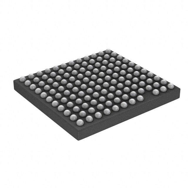
- Part No.:
- CYUSB3014-FBXIT
- Manufacturer:
- Infineon Technologies
- Category:
- Application Specific Microcontrollers
- Package:
- 131-UFBGA, WLCSP
- Datasheet:
-
 CYUSB3014-FBXIT.pdf
- Description:
- IC USB CTLR
- Quantity:
- Payment:

- Shipping:

Inventory:4,544
Please send an inquiry. Send us your inquiry, and we will respond immediately.
Product details
Overview
CYUSB3014-FBXIT from Infineon is a USB 3.2 Gen 1 (5 Gbps) and USB 2.0 programmable SuperSpeed USB controller with ARM926EJ-S CPU (200 MHz), 512 KB SRAM, GPIF II interface (8/16/24/32-bit, 100 MHz), and support for SPI (33 MHz), UART (4 Mbps), I²C (1 MHz), and I²S (up to 192 kHz). It serves as a high-bandwidth bridge between USB hosts and external image sensors, FPGAs, or data acquisition peripherals in embedded vision systems.
For engineers reviewing the CYUSB3014-FBXIT datasheet, CYUSB3014-FBXIT pinout, CYUSB3014-FBXIT application, or CYUSB3014-FBXIT equivalent, key selection criteria include USB 3.2 Gen 1 PHY compliance (TID #340800007), GPIF II configurability for custom parallel interfaces, low-power core mode (<60 µA), independent 1.2 V core / 1.8–3.3 V I/O power domains, and BGA-121 (10 × 10 mm, 0.8 mm pitch) package compatibility with high-density PCB layouts.
Technical Context
The CYUSB3014-FBXIT implements a dual-mode USB controller with fully compliant USB 3.2 Gen 1 (5 Gbps) and USB 2.0 physical layers, including HS-OTG host/peripheral functionality per OTG Supplement v2.0. Its ARM926EJ-S CPU executes firmware directly from on-chip 512 KB SRAM and supports real-time control of 32 physical endpoints.
GPIF II operates at up to 100 MHz with programmable bus widths (8/16/24/32-bit) and 16 configurable control signals, enabling deterministic timing for synchronous/asynchronous slave FIFO, SRAM, or custom logic interfacing - critical for pixel-accurate video streaming from CMOS sensors or FPGA-based frame buffers.
Key Specifications
| Parameter | Value and Actual Design Meaning |
|---|---|
| USB Speed | 5 Gbps SuperSpeed (USB 3.2 Gen 1) + 480 Mbps High-Speed (USB 2.0); enables single-cable HD/4K video transfer without compression. |
| CPU Core | ARM926EJ-S @ 200 MHz; runs real-time firmware for endpoint management, protocol translation, and GPIF II state machine control. |
| On-chip Memory | 512 KB SRAM; sufficient for UVC-compliant video streaming firmware, descriptor tables, and DMA buffer management without external RAM. |
| GPIF II Bus Width | Programmable 8/16/24/32-bit; matches common image sensor output buses (e.g., 16-bit Bayer RAW) or FPGA AXI-stream widths. |
| Power Domains | Independent 1.2 V core / 1.8–3.3 V I/O; allows direct interfacing to 1.8 V FPGAs or 3.3 V sensors without level shifters. |
| Low-Power Mode | <60 µA (VBATT on); supports battery-powered portable imaging devices with USB suspend/resume capability. |
| Clock Inputs | 19.2, 26, 38.4, or 52 MHz crystal or oscillator; 19.2 MHz option aligns with USB SOF timing and common sensor reference clocks. |
Pinout & Package
Package: 121-ball Pb-free BGA, 10 mm × 10 mm, 0.8 mm pitch (ball map per Infineon datasheet Rev. *Z, Table 24 and Section 16).
| Pin/Terminal | Circuit Role | Design Meaning |
|---|---|---|
| USB3_DP / USB3_DM | SuperSpeed differential pair | 5-Gbps USB 3.2 Gen 1 signaling; requires controlled 90-Ω differential impedance routing. |
| USB2_DP / USB2_DM | High-Speed USB 2.0 differential pair | Backward-compatible 480-Mbps signaling; shared physical layer with USB3 lines via multiplexer. |
| GPIF_DATA[31:0] | Configurable parallel data bus | Programmable width (8/16/24/32-bit); connects directly to FPGA GPIO banks or image sensor output buses. |
| GPIF_CTL[15:0] | Configurable control signals | 16 user-defined strobes (e.g., SLRD, SLWR, FLAGA) for handshake timing with external logic. |
| VDD_CORE | Core power supply | 1.2 V ±3%; powers ARM926EJ-S CPU and internal logic; requires low-noise LDO regulation. |
| VDDIO_1 / VDDIO_2 | I/O power supplies | 1.8–3.3 V; independently configurable per bank to match attached peripheral voltage levels. |
Key Features
| Feature | Design Value |
|---|---|
| USB 3.2 Gen 1 PHY Compliance | TID #340800007 certified; ensures interoperability with host controllers and eliminates USB-IF compliance testing risk. |
| GPIF II Programmability | Graphical GPIF II Designer tool generates synthesizable state machines; reduces interface firmware development time by >70% vs. bit-banged GPIO. |
| 32 Physical Endpoints | Supports simultaneous bulk IN/OUT, isochronous video, and control transfers - essential for UVC-compliant multi-stream cameras. |
| Boot Flexibility | Supports boot from SPI flash, I²C EEPROM, or USB host download; enables field firmware updates without JTAG debugger. |
| I²S Master (TX only) | Generates LRCLK/BCLK/SDATA at 8–192 kHz sample rates; drives audio ADCs or digital microphones in multimodal capture systems. |
Applications
| Digital Video Camcorders | Industrial Cameras |
|---|---|
Use Scenario: High-resolution (1080p/4K) video capture with minimal latency and no host-side compression. IC Role / Device Role / Timing Role: USB bridge controller managing pixel data flow from CMOS sensor to host PC via UVC class driver. Use Value: GPIF II configured as 16-bit synchronous slave FIFO delivers sustained 300+ MB/s throughput - matching USB 3.2 Gen 1 theoretical bandwidth. | Use Scenario: Machine vision inspection system requiring precise trigger synchronization and multi-camera timestamp alignment. IC Role / Device Role / Timing Role: Deterministic USB interface with hardware timestamping and GPIO-triggered frame capture. Use Value: Independent 32-kHz watchdog clock input enables sub-millisecond timestamp resolution across distributed camera nodes. |
| Medical Imaging Devices | Surveillance Cameras |
Use Scenario: Portable ultrasound or endoscopy probe transmitting uncompressed real-time video over USB. IC Role / Device Role / Timing Role: Low-latency USB 3.2 Gen 1 endpoint with integrated SRAM buffering and power-managed idle states. Use Value: Core power-down mode draws <60 µA during standby - extends battery life in handheld diagnostic tools. | Use Scenario: IP-based security camera with local video analytics and USB-connected storage or host upload. IC Role / Device Role / Timing Role: Dual-role USB device supporting both UVC streaming and mass-storage-class recording to USB flash drive. Use Value: HS-OTG host/peripheral capability enables seamless switching between camera mode and storage mode without hardware reconfiguration. |
Equivalent & Alternatives
The following parts are listed as comparable options for similar USB 3.0 bridge controller applications.
| Alternative Part | Technical Difference | Application Difference | Selection Advice |
|---|---|---|---|
| CYUSB3014-BZXI | Same silicon; 121-ball BGA but with leaded (Pb) finish and industrial temperature range (–40°C to +85°C) vs. CYUSB3014-FBXIT's commercial grade (0°C to +70°C). | Required for extended-temperature deployments (e.g., outdoor surveillance, factory-floor imaging). | Select when RoHS exemption for leaded solder is approved and ambient operating temperature exceeds 70°C. |
| CX3-EBZ | Dedicated MIPI CSI-2 to USB 3.0 bridge (no ARM CPU, no GPIF II); fixed-function, lower BOM cost. | Suitable only for MIPI-based image sensors; lacks programmability for non-MIPI interfaces like parallel LVDS or FPGA custom protocols. | Choose for cost-sensitive, MIPI-only camera modules where firmware customization is unnecessary. |
Compared with CYUSB3014-BZXI, the FBXIT variant offers RoHS-compliant packaging and commercial-temperature operation - ideal for consumer and lab-grade prototyping; versus CX3-EBZ, it provides full firmware programmability and parallel interface flexibility at higher component count and design effort.
Availability
CYUSB3014-FBXIT is available at Aetrix Electronics and suitable for digital video camcorders, industrial machine vision systems, and medical imaging devices requiring stable component supply and long-term production continuity.
Supply support for CYUSB3014-FBXIT includes scheduled delivery planning, volume procurement assistance, BOM continuity management, traceable sourcing, and lifecycle availability coordination for OEM customers, industrial embedded developers, connected-device designers, and electronics production programs.
Manufacturer
Infineon Technologies is a German semiconductor manufacturer specializing in power management, automotive ICs, and connectivity solutions, with global R&D and manufacturing infrastructure.
The EZ-USB FX3 product line targets high-bandwidth embedded USB bridging applications - specifically enabling lossless video, sensor fusion, and FPGA-hosted data acquisition systems requiring deterministic USB 3.2 Gen 1 performance.
FAQ
Does CYUSB3014-FBXIT require an external crystal?
Yes - it supports 19.2, 26, 38.4, or 52 MHz crystal or oscillator inputs. A 19.2 MHz crystal is recommended for USB SOF timing accuracy and compatibility with common image sensor reference clocks. The device integrates internal PLLs to generate required USB and CPU clocks from this input.
Can CYUSB3014-FBXIT operate as a USB host?
Yes - it implements USB On-The-Go (OTG) Supplement v2.0, enabling HS-OTG host mode to enumerate and control USB peripherals such as flash drives, HID devices, or serial adapters. Host mode requires appropriate VBUS control circuitry and firmware-level USB host stack integration.
What development tools are included with the EZ-USB FX3 SDK?
The official Infineon EZ-USB FX3 SDK includes ThreadX RTOS framework, firmware examples for all I/O modules (SPI, UART, I²C, I²S, GPIF II), Visual Studio host applications in C++/C#, GPIF II Designer GUI tool, and USB descriptor configuration utilities - all provided royalty-free for commercial use.
Is JTAG debugging supported on CYUSB3014-FBXIT?
Yes - the device features a dedicated 5-pin JTAG interface (TCK, TMS, TDI, TDO, TRST#) compliant with IEEE 1149.1, enabling full boundary-scan testing, CPU core debugging, and firmware flash programming using standard tools like Segger J-Link or Infineon's MiniProg3.
CYUSB3014-FBXIT Specifications
- Product attributes
- Attribute value
- Manufacturer:
- Infineon Technologies
- Series:
- EZ-USB FX3™
- Package/Case:
- 131-UFBGA, WLCSP
- Packaging:
- Tape & Reel (TR)
- Product Status:
- Obsolete
- Programmable:
- Not Verified
- Applications:
- SuperSpeed USB Peripheral Controller
- Core Processor:
- ARM9®
- Program Memory Type:
- External Program Memory
- Controller Series:
- CYUSB
- RAM Size:
- 512K x 8
- Interface:
- GPIF, I2C, I2S, SPI, UART, USB
- Number of I/O:
- 60
- Voltage - Supply:
- 1.15V ~ 1.25V
- Operating Temperature:
- -40°C ~ 85°C
- Grade:
- -
- Qualification:
- -
- Mounting Type:
- Surface Mount
- Supplier Device Package:
- 131-WLCSP (5.1x4.7)
CYUSB3014-FBXIT FAQ
1.How can I place an order for CYUSB3014-FBXIT through Aetrix?
Please submit a Request for Quotation (RFQ) for CYUSB3014-FBXIT on Aetrix. Our sales agent will provide a competitive quotation and guide you through the order confirmation once you accept the terms.
2.Are the price and stock information for CYUSB3014-FBXIT reliable?
The price and inventory of CYUSB3014-FBXIT are updated periodically and may fluctuate due to market conditions. Stock and pricing data are typically refreshed every 24 hours. Quotation validity for CYUSB3014-FBXIT is usually 5 days.
3.What payment methods are accepted for CYUSB3014-FBXIT?
We accept Wire Transfer, PayPal, Credit Card, Western Union, MoneyGram, and Escrow for CYUSB3014-FBXIT transactions.
Note: Certain payment methods may incur a processing fee.
4.How is shipping managed for CYUSB3014-FBXIT?
CYUSB3014-FBXIT orders can be shipped via leading logistics carriers, including DHL, UPS, FedEx, TNT, or Registered Mail.
Once your CYUSB3014-FBXIT order is processed, you will receive an email with the shipment details and tracking number.
Note: Tracking information may take up to 24 hours to appear. Express delivery typically takes 3–5 business days.
5.How can I obtain technical support or documentation for CYUSB3014-FBXIT?
For technical support, including CYUSB3014-FBXIT datasheets, pinout diagrams, or application guidance, please contact our engineering support team. They can provide detailed documentation and assistance for your CYUSB3014-FBXIT requirements.
6.How does Aetrix verify that CYUSB3014-FBXIT is sourced from the original manufacturer or authorized distributors?
All CYUSB3014-FBXIT products on Aetrix are procured from qualified distributors and authorized channels. Our dedicated quality assurance team conducts strict verification, including traceability checks and, if necessary, third-party testing. This ensures that CYUSB3014-FBXIT meets industry standards.
7.What is the process for return or replacement of CYUSB3014-FBXIT?
All CYUSB3014-FBXIT units undergo pre-shipment inspection (PSI). If there is an issue with CYUSB3014-FBXIT, returns or replacements are accepted under the following conditions:
1.Quantity discrepancies, incorrect items, or visible external defects (such as breakage or corrosion), acknowledged by Aetrix.
2.The issue is reported within 90 days of delivery.
3.The CYUSB3014-FBXIT part is unused and in its original packaging.
Return procedure for CYUSB3014-FBXIT:
1.Submit a request within 90 days.
2.Obtain a Return Material Authorization (RMA) from Aetrix.
CYUSB3014-FBXIT Tags

-
CYPD3175-24LQXQ
Infineon Technologies

-
SLB9672VU20FW1523XTMA1
Infineon Technologies

-
SLB9670VQ20FW785XTMA1
Infineon Technologies
-
SLB9672XU20FW1523XTMA1
Infineon Technologies
-
SLB9673XU20FW2613XTMA1
Infineon Technologies

-
CYPD3125-40LQXIT
Infineon Technologies

-
AT97SC3204-U2A1A-20
Microchip Technology
-
AT97SC3204-U2A1A-10
Microchip Technology
-
SLM9670AQ20FW1311XTMA1
Infineon Technologies
-
SLB9672XU20FW1613XTMA1
Infineon Technologies
-
SLB9672AU20FW1613XTMA1
Infineon Technologies
-
SLB9673AU20FW2613XTMA1
Infineon Technologies
Tech Hub

Operational amplifier guide covering op amp basics, feedback, ideal vs real op amps, common configurations, buffer circuits, offset, bias current, gain-bandwidth, slew rate, rail-to-rail limits and sel…

Jumper cables guide covering safe connection order, red and black clamp placement, final ground connection, cable gauge, length, clamp quality, copper vs CCA cables, jump starter comparison and battery…

LDO regulator guide covering low dropout voltage, power dissipation, thermal design, PSRR, output noise, capacitor stability, adjustable LDO circuits, LDO vs buck converter and datasheet selection chec…

Conditional Access Module guide covering CAM meaning, CI/CI+ interface, smart card authorization, DVB security workflow, TV and set-top box compatibility, internal electronics, ESD protection, connecto…

Guide to electronic component obsolescence covering EOL risk, PCN/PDN notices, last-time buy planning, replacement options, form-fit-function validation, counterfeit risk and BOM lifecycle management.

18650 battery guide covering lithium-ion cell basics, 3.6V/3.7V voltage, 4.2V charging, mAh and Wh capacity, protected cells, chargers, BMS, series-parallel packs, holders, welding and sourcing checks.…

Hall effect sensor guide covering working principle, linear and digital sensors, Arduino circuits, current sensing, speed detection, automotive applications, A3144 examples, signal filtering and datash…

Product Change Notification guide for electronic components, covering PCN meaning, PCN vs PDN/EOL, common change types, risk levels, form-fit-function review, engineering validation, BOM control, LTB/L…

A practical guide to blend door actuators, covering HVAC function, symptoms, location, AC and heater issues, reset and calibration, replacement cost, electrical diagnosis, compatibility checks, and rep…

Engineering guide to Raspberry Pi alternatives, covering chip-level differences, Orange Pi, ROCK, Jetson, Banana Pi, NanoPi, Compute Module, Pico, GPIO, camera, HAT compatibility, and replacement risks…


