
 My Inquiry
 My Account


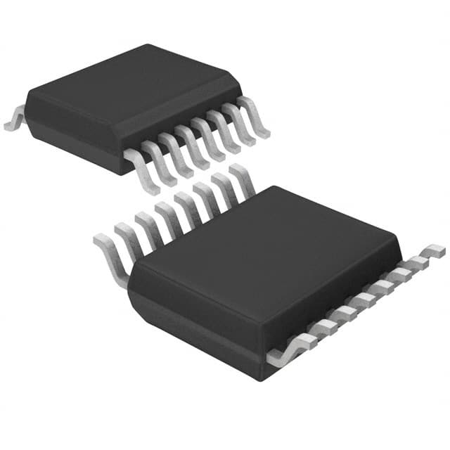
Renesas EL7457CUZ-T7A
- Part No.:
- EL7457CUZ-T7A
- Manufacturer:
- Renesas
- Category:
- Gate Drivers
- Package:
- 16-SSOP (0.154", 3.90mm Width)
- Datasheet:
-
 EL7457CUZ-T7A.pdf
- Description:
- IC GATE DRVR HI/LOW SIDE 16QSOP
- Quantity:
- Payment:

- Shipping:

Inventory:250
Please send an inquiry. Send us your inquiry, and we will respond immediately.
Product details
Overview
EL7457CUZ-T7A from Renesas Electronics is a 40MHz non-inverting quad CMOS driver IC with 2A peak output current, 3Ω typical on-resistance, and matched rise/fall times within 1ns-designed for driving high-capacitance CCD storage/vertical clocks in digital camera systems.
For engineers reviewing the EL7457CUZ-T7A datasheet, EL7457CUZ-T7A pinout, EL7457CUZ-T7A application, or EL7457CUZ-T7A equivalent, key selection criteria include dual-supply operation (–5V to +16.5V), TTL/CMOS-compatible inputs, fast 12ns enable/disable timing, and QSOP-16 packaging optimized for space-constrained imaging and ATE pin-driver designs.
Technical Context
The EL7457CUZ-T7A integrates four independent high-side (P-channel) and low-side (N-channel) drivers sharing common VH and VL rails, enabling rail-to-rail output switching between programmable voltage levels. Each channel operates with ground-referenced logic inputs and supports single- or dual-supply configurations.
Its internal architecture delivers tightly matched propagation delays (≤2ns mismatch), 12ns output enable/disable response, and <1mA quiescent current-critical for synchronized multi-channel clock distribution in CCD and ultrasound transducer driver applications where timing skew must be minimized.
Key Specifications
| Parameter | Value and Actual Design Meaning |
|---|---|
| Max Clock Rate | 40MHz - supports high-speed vertical/horizontal clocking in CCD image sensors |
| Peak Output Current | 2A - drives heavy capacitive loads up to 1000pF with minimal droop |
| On-Resistance | 3Ω nominal - ensures low conduction loss and thermal stability under 100mA continuous load |
| Rise/Fall Time Match | ≤1ns - maintains signal integrity across all four channels in time-critical applications |
| Enable/Disable Delay | 12ns - enables rapid power-down sequencing during CCD blanking intervals |
| Supply Voltage Range | VH = –2V to +16.5V, VL = –5V to +8V - supports wide-range level-shifting for mixed-voltage systems |
| Input Compatibility | 3V/5V CMOS and TTL - simplifies interface with FPGA, ASIC, or microcontroller control logic |
Pinout & Package
EL7457CUZ-T7A is housed in a RoHS-compliant 16-pin QSOP (0.150") package (MDP0040), featuring exposed thermal pad connection to VS− and optimized lead pitch for automated assembly in high-density PCB layouts.
| Pin/Terminal | Circuit Role | Design Meaning |
|---|---|---|
| 1 (INA) | Channel A input | Ground-referenced CMOS/TTL logic input controlling OUTA |
| 2 (OE) | Global output enable | Active-low signal placing all four outputs in high-impedance state |
| 3 (INB) | Channel B input | Ground-referenced CMOS/TTL logic input controlling OUTB |
| 4 (VL) | Low-side supply rail | Defines lower output voltage limit (–5V to +8V); shared across all channels |
| 5 (GND) | Logic ground reference | Reference for all input signals; isolated from power supply return paths |
| 7 (INC) | Channel C input | Ground-referenced CMOS/TTL logic input controlling OUTC |
| 8 (IND) | Channel D input | Ground-referenced CMOS/TTL logic input controlling OUTD |
| 9 (VS−) | Negative supply voltage | Power rail for internal circuitry; connected to thermal pad for heat dissipation |
| 10 (OUTD) | Channel D output | Switched between VH and VL based on IND; capable of 2A peak sink/source |
| 11 (OUTC) | Channel C output | Switched between VH and VL based on INC; matched timing with other outputs |
| 12 (VH) | High-side supply rail | Defines upper output voltage limit (–2V to +16.5V); shared across all channels |
| 14 (OUTB) | Channel B output | Switched between VH and VL based on INB; 3Ω on-resistance minimizes voltage drop |
| 15 (OUTA) | Channel A output | Switched between VH and VL based on INA; supports 40MHz toggle rate into 1000pF |
| 16 (VS+) | Positive supply voltage | Power rail for internal circuitry; decoupling required per datasheet layout guidelines |
Key Features
| Feature | Design Value |
|---|---|
| Quad-channel rail-to-rail drive | Four independent outputs switch between user-defined VH and VL rails-enabling flexible level-shifting without external translators |
| Tight timing matching | Rise/fall time mismatch ≤1ns and propagation delay mismatch ≤2ns ensure sub-nanosecond inter-channel skew for precision timing |
| Fast enable/disable control | 12ns OE response allows dynamic channel disabling during CCD power-down cycles without signal corruption |
| Wide dual-supply range | Supports VS+ to VS− up to 18V with independent VH/VL programming-ideal for mixed-signal imaging and ultrasonic generator biasing |
| Low quiescent current | <1mA supply current at idle reduces system-level power budget impact in always-on sensor interfaces |
Applications
| CCD Image Sensor Clocking | Digital Camera Vertical Drive |
|---|---|
Use Scenario: Driving vertical shift register clocks in interline-transfer CCDs requiring precise 40MHz timing and high capacitive load handling. IC Role / Device Role / Timing Role: Quad CMOS driver providing synchronized, rail-to-rail clock edges to CCD vertical registers with matched propagation delay. Use Value: 1ns rise/fall match and 2ns prop delay match eliminate vertical smearing by ensuring pixel row activation alignment across all four clock phases. | Use Scenario: Generating high-current vertical drive pulses in compact digital cameras where board space limits discrete driver solutions. IC Role / Device Role / Timing Role: Integrated quad driver replacing four discrete MOSFETs, reducing layout area and parasitic inductance in tight camera modules. Use Value: 2A peak current and 3Ω on-resistance deliver clean 1000pF load transitions at full frame rate, minimizing vertical line distortion. |
| ATE Pin Driver | Ultrasound Transducer Excitation |
Use Scenario: Driving DUT pins in automated test equipment requiring fast, repeatable voltage transitions and high channel density. IC Role / Device Role / Timing Role: High-speed level-shifting driver translating tester logic levels to device-under-test interface voltages with minimal skew. Use Value: 12ns enable/disable and 40MHz max clock rate support high-throughput parametric testing with deterministic timing windows. | Use Scenario: Generating bipolar excitation waveforms for piezoelectric ultrasound transducers in portable medical imaging systems. IC Role / Device Role / Timing Role: Dual-rail driver delivering phase-matched positive/negative pulses to transducer elements via VH/VL configuration. Use Value: Independent VH (up to +16.5V) and VL (down to –5V) rails enable ±12V pulse generation with <1ns edge matching for improved axial resolution. |
Equivalent & Alternatives
The following parts are listed as comparable options for similar quad high-speed driver applications.
| Alternative Part | Technical Difference | Application Difference | Selection Advice |
|---|---|---|---|
| EL7457CSZ-T7A | Same die, SOIC-16 package (MDP0027); higher θJA (73°C/W) vs QSOP's 112°C/W | Better thermal performance in high-power-density layouts; larger footprint than QSOP | Select when board-level thermal management prioritizes lower junction temperature over size |
| EL7457CLZ-T7A | Same die, QFN-16 (4×4mm) package; lowest θJA (43°C/W) and smallest footprint | Requires careful PCB thermal pad design; not compatible with through-hole assembly | Select for ultra-compact, thermally demanding applications like handheld ultrasound probes |
Compared with EL7457CUZ-T7A, the SOIC variant offers easier hand-soldering and legacy compatibility, while the QFN variant delivers superior thermal efficiency and miniaturization-both share identical electrical specs and timing behavior but differ in mechanical integration requirements.
Availability
EL7457CUZ-T7A is available at Aetrix Electronics and suitable for CCD clocking, digital camera vertical drive, and ATE pin-driving applications requiring stable component supply, consistent parametric performance, and long-term industrial availability.
Supply support for EL7457CUZ-T7A includes scheduled delivery planning, volume procurement assistance, BOM continuity management, traceable sourcing, and lifecycle availability coordination for OEM customers, industrial embedded developers, connected-device designers, and electronics production programs.
Manufacturer
Renesas Electronics Corporation is a global semiconductor leader specializing in microcontrollers, analog, power, and SoC solutions for automotive, industrial, and IoT markets.
The EL7457CUZ-T7A belongs to Renesas' high-speed driver product line, engineered specifically for precision timing-critical applications including CCD/CMOS image sensors, medical ultrasound, and automated test equipment.
FAQ
What is the maximum operating frequency supported by the EL7457CUZ-T7A?
The EL7457CUZ-T7A supports clock rates up to 40MHz, verified under standard test conditions with 1000pF load capacitance. This rating applies across the full –40°C to +85°C ambient temperature range and is enabled by its 12ns rise/fall times and matched propagation characteristics. The EL7457CUZ-T7A maintains this performance with both 3V and 5V logic inputs, making it suitable for high-speed CCD clocking and ATE applications where timing fidelity is critical.
How does the EL7457CUZ-T7A handle level shifting between different voltage domains?
The EL7457CUZ-T7A implements level shifting through independent VH and VL supply pins, allowing outputs to swing between user-defined high and low voltage rails-ranging from –5V to +16.5V for VH and –5V to +8V for VL. Inputs remain ground-referenced and compatible with 3V/5V CMOS or TTL logic. This architecture enables the EL7457CUZ-T7A to translate control signals into arbitrary output voltage ranges without external components, supporting applications like ultrasound transducer excitation and mixed-voltage sensor interfaces.
What is the purpose of the OE (output enable) pin on the EL7457CUZ-T7A?
The OE pin on the EL7457CUZ-T7A is an active-low global control that places all four outputs in a high-impedance state within 12ns of assertion. This function is essential in CCD applications during power-down sequences to prevent unintended charge injection or bus contention. The EL7457CUZ-T7A's fast enable/disable timing ensures clean transitions without overshoot or timing skew, preserving signal integrity across all channels simultaneously.
Can the EL7457CUZ-T7A operate from a single supply, and what are the constraints?
Yes, the EL7457CUZ-T7A supports single-supply operation-for example, with VS+ = +15V and VS− = 0V-while maintaining full functionality. In this configuration, VH must be ≤ VS+ and VL ≥ VS−, and the VH–VL differential must remain within 0V to 16.5V. Input logic remains ground-referenced, and the EL7457CUZ-T7A retains its 2A peak drive capability and 3Ω on-resistance. However, thermal performance must be validated per the SOIC/QSOP/QFN θJA values, as power dissipation increases with larger voltage swings.
What package type does the EL7457CUZ-T7A use, and how does it affect thermal performance?
The EL7457CUZ-T7A uses a 16-pin QSOP (0.150") package (MDP0040) with θJA = 112°C/W and θJC = N/A. While less thermally efficient than the QFN variant (θJA = 43°C/W), the QSOP offers robust manufacturability, compatibility with standard reflow profiles, and ease of inspection. Its thermal pad is internally connected to VS−, requiring appropriate PCB copper pour for heat dissipation. For EL7457CUZ-T7A deployments exceeding 1W power dissipation, thermal simulation using the provided θJA value is recommended to ensure TJ remains below 125°C.
EL7457CUZ-T7A Specifications
- Product attributes
- Attribute value
- Manufacturer:
- Renesas
- Series:
- -
- Package/Case:
- 16-SSOP (0.154", 3.90mm Width)
- Packaging:
- Tape & Reel (TR)
- Product Status:
- Active
- Programmable:
- Not Verified
- Driven Configuration:
- High-Side or Low-Side
- Channel Type:
- Independent
- Number of Drivers:
- 4
- Gate Type:
- N-Channel, P-Channel MOSFET
- Voltage - Supply:
- 4.5V ~ 18V
- Logic Voltage - VIL, VIH:
- 0.8V, 2V
- Current - Peak Output (Source, Sink):
- 2A, 2A
- Input Type:
- Non-Inverting
- High Side Voltage - Max (Bootstrap):
- -
- Rise / Fall Time (Typ):
- 13.5ns, 13ns
- Operating Temperature:
- -40°C ~ 85°C (TA)
- Grade:
- -
- Qualification:
- -
- Mounting Type:
- Surface Mount
- Supplier Device Package:
- 16-QSOP
EL7457CUZ-T7A FAQ
1.How can I place an order for EL7457CUZ-T7A through Aetrix?
Please submit a Request for Quotation (RFQ) for EL7457CUZ-T7A on Aetrix. Our sales agent will provide a competitive quotation and guide you through the order confirmation once you accept the terms.
2.Are the price and stock information for EL7457CUZ-T7A reliable?
The price and inventory of EL7457CUZ-T7A are updated periodically and may fluctuate due to market conditions. Stock and pricing data are typically refreshed every 24 hours. Quotation validity for EL7457CUZ-T7A is usually 5 days.
3.What payment methods are accepted for EL7457CUZ-T7A?
We accept Wire Transfer, PayPal, Credit Card, Western Union, MoneyGram, and Escrow for EL7457CUZ-T7A transactions.
Note: Certain payment methods may incur a processing fee.
4.How is shipping managed for EL7457CUZ-T7A?
EL7457CUZ-T7A orders can be shipped via leading logistics carriers, including DHL, UPS, FedEx, TNT, or Registered Mail.
Once your EL7457CUZ-T7A order is processed, you will receive an email with the shipment details and tracking number.
Note: Tracking information may take up to 24 hours to appear. Express delivery typically takes 3–5 business days.
5.How can I obtain technical support or documentation for EL7457CUZ-T7A?
For technical support, including EL7457CUZ-T7A datasheets, pinout diagrams, or application guidance, please contact our engineering support team. They can provide detailed documentation and assistance for your EL7457CUZ-T7A requirements.
6.How does Aetrix verify that EL7457CUZ-T7A is sourced from the original manufacturer or authorized distributors?
All EL7457CUZ-T7A products on Aetrix are procured from qualified distributors and authorized channels. Our dedicated quality assurance team conducts strict verification, including traceability checks and, if necessary, third-party testing. This ensures that EL7457CUZ-T7A meets industry standards.
7.What is the process for return or replacement of EL7457CUZ-T7A?
All EL7457CUZ-T7A units undergo pre-shipment inspection (PSI). If there is an issue with EL7457CUZ-T7A, returns or replacements are accepted under the following conditions:
1.Quantity discrepancies, incorrect items, or visible external defects (such as breakage or corrosion), acknowledged by Aetrix.
2.The issue is reported within 90 days of delivery.
3.The EL7457CUZ-T7A part is unused and in its original packaging.
Return procedure for EL7457CUZ-T7A:
1.Submit a request within 90 days.
2.Obtain a Return Material Authorization (RMA) from Aetrix.
EL7457CUZ-T7A Tags

-
ZXGD3009E6TA
Diodes Incorporated
-
1EDN7512BXTSA1
Infineon Technologies

-
UCC27517DBVR
Texas Instruments

-
MCP1416T-E/OT
Microchip Technology
-
MCP1402T-E/OT
Microchip Technology
-
MCP1415T-E/OT
Microchip Technology
-
MCP1401T-E/OT
Microchip Technology
-
IX4428NTR
Littelfuse Inc.

-
IRS2005STRPBF
Infineon Technologies
-
IRS2008STRPBF
Infineon Technologies
-
IX4310TTR
Littelfuse Inc.

-
2EDN7524RXTMA1
Infineon Technologies
Tech Hub

TTL and CMOS logic families differ in thresholds, loading, output drive, power and timing. This engineering guide compares 74HC and 74HCT, calculates noise margins and checks 3.3 V/5 V compatibility.

A practical engineering guide to 3.3V and 5V logic compatibility, input thresholds, resistor dividers, translator ICs, MOSFET level shifting, I2C pull-ups, timing limits and power-sequencing risks.

The 74HC595 uses push-pull logic outputs, while the TPIC6B595 uses 50 V open-drain DMOS sinks for higher-power loads. This guide compares timing, current limits, 3.3 V interfacing, load wiring, thermal…

The 74HC595 converts serial data into eight stable parallel outputs. This guide covers pin functions, shift and storage timing, OE and MR behavior, drive-current limits, cascading, voltage compatibilit…

A technical comparison of level-sensitive latches and edge-triggered flip-flops, covering timing windows, setup and hold limits, master–slave operation, time borrowing, race-through, HDL inference and…

A D latch stores one bit while Enable controls when data can pass. This reference covers gate-level operation, truth tables, transparency, setup and hold timing, LE versus OE, common ICs and practical …

An SR latch stores one bit through cross-coupled feedback. This engineering reference covers NOR and NAND implementations, truth tables, forbidden-state recovery, gated operation, switch debouncing, fa…

Latch circuits retain one bit through feedback. This technical reference covers SR and D latches, truth tables, transparency, timing limits, latch-versus-flip-flop behavior, applications and common log…

An engineering guide to LED driver operation, constant-current and constant-voltage outputs, linear and switching topologies, dimming, IC selection, calculations, replacement compatibility, and fault c…

Operational amplifier guide covering op amp basics, feedback, ideal vs real op amps, common configurations, buffer circuits, offset, bias current, gain-bandwidth, slew rate, rail-to-rail limits and sel…


