
 My Inquiry
 My Account


Analog Devices Inc. HMC920LP5E
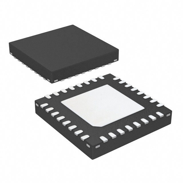
- Part No.:
- HMC920LP5E
- Manufacturer:
- Analog Devices Inc.
- Category:
- Power Management - Specialized
- Package:
- 32-VFQFN Exposed Pad
- Datasheet:
-
 HMC920LP5E.pdf
- Description:
- IC CTRLR ACTIVE BIAS 32QFN
- Quantity:
- Payment:

- Shipping:

Inventory:4,612
Please send an inquiry. Send us your inquiry, and we will respond immediately.
Product details
Overview
HMC920LP5E from Analog Devices is an active bias controller IC designed to regulate drain voltage and dynamically adjust gate voltage for RF power amplifiers, enabling stable Class-A biasing across temperature, supply, and process variation. It supports 3V–15V adjustable VDRAIN, up to 500mA drain current, and integrates an internal −2.5V negative voltage generator - used in cellular base stations and microwave radio transceivers to maintain amplifier linearity and efficiency.
For engineers reviewing the HMC920LP5E datasheet, HMC920LP5E pinout, HMC920LP5E application, or HMC920LP5E equivalent, key selection considerations include its dual-domain supply architecture (Vdd/VDIG), active current regulation loop, programmable over/under-current alarm thresholds, and daisy-chain trigger-out sequencing capability for multi-amplifier bias systems.
Technical Context
The HMC920LP5E implements a closed-loop active bias control architecture that continuously samples IDRAIN via an external sense resistor and adjusts VGATE (±4 mA sourcing/sinking) to hold constant quiescent current - independent of amplifier threshold drift, aging, or thermal shift. Its high-voltage LDO (LDOCC) delivers up to 500 mA at 3–15 V with <0.05%/V line regulation and <0.008%/°C temperature drift.
It features two isolated voltage domains: a 5–16.5 V high-side domain (Vdd1/Vdd2) powering the LDOCC and charge pump, and a 3.5 V low-side digital domain (VDIG) supplying logic, oscillator, and control blocks. The integrated −2.5 V charge-pump generator (VNEG) supports depletion-mode FET biasing and is disableable via VNEGFB/VVGATEFB pin configuration.
Key Specifications
| Parameter | Value and Actual Design Meaning |
|---|---|
| Supply Voltage Range | 5 V to 16.5 V - powers both high-voltage LDOCC and internal charge pump; enables direct use with common RF system rails. |
| VDRAIN Output Range | 3 V to 15 V - adjustable via external resistor divider on LDOFB; compensates for 0.5 Ω RDS-ON drop between LDOCC and VDRAIN pins. |
| Max Drain Current | 500 mA - continuous output capability with power foldback protection limiting instantaneous dissipation to ≤4.5 W under short-circuit conditions. |
| VGATE Drive Capability | ±4 mA - sufficient to actively regulate gate voltage of GaAs pHEMT or GaN HEMT amplifiers during large-signal operation and thermal transients. |
| Negative Voltage Output | −2.5 V @ 60 mA sink - internally generated for depletion-mode device bias; disableable to reduce power and simplify layout when not required. |
| Operating Temperature | −40 °C to +85 °C - specified performance across full industrial range, with <0.03 %/°C IDRAIN drift and <0.008 %/°C VDRAIN drift. |
| Package | 5 mm × 5 mm QFN-32 with exposed thermal pad - RoHS-compliant, MSL1 rated, optimized for RF amplifier board integration and thermal management. |
Pinout & Package
Package: 32-lead, 5 mm × 5 mm, RoHS-compliant leadless QFN with exposed backside thermal pad (MSL1, peak reflow 260 °C). Thermal resistance θJ-PAD = 3.9 °C/W.
| Pin/Terminal | Circuit Role | Design Meaning |
|---|---|---|
| Vdd1, Vdd2 (Pins 1, 2, 14) | High-voltage bias supply inputs | Must be tied together and decoupled locally; powers LDOCC, charge pump, and internal regulators - violation risks latch-up or permanent damage. |
| VDRAIN (Pins 22, 23) | Regulated drain supply output | Delivers final bias voltage to amplifier drain; includes internal 0.5 Ω switch - requires ≥100 nF local ceramic bypass near amplifier. |
| VGATE (Pin 21) | Active gate voltage control output | Sources/sinks ±4 mA to stabilize amplifier IQ; requires 10 µF capacitor to AGND at amplifier gate for stability and noise rejection. |
| ISENSE (Pin 25) | Bias current sensing input | Connects to ground via precision Rsense (e.g., 0.5%, ±25 ppm); sets target IDRAIN per IDRAIN = 13.5 mA + 165 Ω / RSENSE. |
| TRGOUT (Pin 24) | Power-sequencing trigger output | Drives HIGH (3.5 V) after bias stabilization - enables daisy-chained enable of downstream HMC920LP5E units without external timing circuitry. |
| EN (Pin 7) | Active bias control enable | Pull to VDIG (≥3.5 V) to activate VGATE/VDRAIN loop; floating defaults to enabled; pull to GND disables outputs and discharges VDRAIN. |
Key Features
| Feature | Design Value |
|---|---|
| Automated power-up sequencing | Internally controls VNEG → VGATE → VDRAIN ramp to prevent amplifier turn-on stress; eliminates need for external sequencer ICs or discrete timers. |
| Stable bias over aging and process | Eliminates factory calibration by maintaining <±0.5% IDRAIN accuracy across lifetime - critical for deployed microwave radios where field recalibration is impractical. |
| Short-circuit protection with power foldback | Reduces VDRAIN and IDRAIN simultaneously under overload to limit package power to ≤4.5 W - avoids thermal runaway while preserving amplifier functionality. |
| Adjustable over/under-current alarm | Three-pin resistor network (ALML/ALMM/ALMH) sets precise trip thresholds - enables system-level fault response (e.g., shutdown, flag, or gain reduction) without firmware intervention. |
| Dual-domain isolation | Separate Vdd (5–16.5 V) and VDIG (3.5 V) domains prevent noise coupling from high-power LDO into sensitive control logic - improves long-term reliability in dense RF layouts. |
Applications
| Cellular Base Station Power Amplifier Bias | Microwave Radio Transmitter Bias |
|---|---|
|
Use Scenario: Biasing GaN HEMT power amplifiers in 4G/5G macrocell remote radio heads operating at ambient temperatures from −40 °C to +65 °C. IC Role / Device Role / Timing Role: Active bias controller providing regulated VDRAIN and adaptive VGATE to maintain constant IQ despite thermal cycling and component aging. Use Value: Enables >10-year field life without recalibration, reduces adjacent-channel leakage ratio (ACLR) drift by >8 dB over temperature, and supports 500 mA peak current for 20W POUT stages. |
Use Scenario: Stabilizing Class-A bias in Ku-band VSAT transmit chains exposed to wide supply variation (12 V ±15%) and rapid thermal transients. IC Role / Device Role / Timing Role: Regulates amplifier quiescent current using real-time ISENSE feedback and dynamic VGATE adjustment, synchronized with TRGOUT-triggered PA enable. Use Value: Maintains EVM <2.5% across −40 °C to +85 °C and ±10% Vdd variation, eliminates manual trim during production, and supports daisy-chained multi-stage biasing with single control signal. |
| Military Radar T/R Module Bias | Test Instrumentation Amplifier Bias |
|
Use Scenario: Biasing high-reliability GaAs pHEMT amplifiers in airborne radar T/R modules requiring MIL-STD-810H environmental compliance and zero field maintenance. IC Role / Device Role / Timing Role: Provides fault-tolerant bias with VddALM undervoltage detection and CURALM overcurrent signaling - integrated into system health monitoring via ALMTRIG test interface. Use Value: Guarantees amplifier turn-on only after full stabilization (TRGOUT assertion), prevents gate oxide stress during cold start, and enables automated self-test via ALMTRIG pin. |
Use Scenario: Precision biasing of broadband RF amplifiers in vector network analyzers and signal generators where measurement repeatability demands sub-0.1% IQ stability. IC Role / Device Role / Timing Role: Delivers ultra-stable VDRAIN (0.008 %/°C drift) and VGATE with active current regulation - referenced to internal 2 V bandgap (±2% accuracy). Use Value: Reduces measurement drift to <0.02 dB amplitude error over 8-hour calibration cycles, supports fast sweep modes via EN-controlled on/off, and enables traceable bias settings via external Rsense programming. |
Equivalent & Alternatives
The following parts are listed as comparable options for similar active bias controller applications.
| Alternative Part | Technical Difference | Application Difference | Selection Advice |
|---|---|---|---|
| LM3478MM/NOPB | Step-down DC/DC controller (no integrated LDO, no VGATE loop, no negative voltage generation) | Requires external op-amp current loop, discrete gate driver, and separate −VSS supply - adds 12+ components and layout complexity | Only suitable if system already provides −VSS, has dedicated analog control resources, and tolerates higher design risk and calibration burden. |
| MAX2034ETA+ | RF power detector + comparator-based bias IC (no active VGATE adjustment, no LDOCC, no TRGOUT) | Lacks closed-loop regulation - relies on fixed gate voltage and open-loop drain supply; cannot compensate for aging or thermal drift | Acceptable only for non-critical, low-power (<100 mA), room-temperature lab setups where long-term stability is not required. |
Compared with LM3478MM/NOPB and MAX2034ETA+, the HMC920LP5E delivers fully integrated, self-contained active bias control - eliminating external compensation networks, reducing BOM count by ≥15 components, and guaranteeing ±0.5% IDRAIN stability over temperature, supply, and 10-year operational life without recalibration.
Availability
HMC920LP5E is available at Aetrix Electronics and suitable for cellular infrastructure, microwave radio, and military radar applications requiring stable component supply, long-lifecycle support, and guaranteed RoHS-compliant manufacturing.
Supply support for HMC920LP5E includes scheduled delivery planning, volume procurement assistance, BOM continuity management, traceable sourcing, and lifecycle availability coordination for OEM customers, industrial embedded developers, connected-device designers, and electronics production programs.
Manufacturer
Analog Devices, Inc. is a global leader in high-performance analog, mixed-signal, and RF technologies, serving communications, industrial, automotive, and defense markets with precision signal processing solutions.
The HMC920LP5E belongs to Analog Devices' Hittite Microwave product line - engineered specifically for RF power amplifier biasing in demanding wireless infrastructure and aerospace applications where stability, integration, and reliability are non-negotiable.
FAQ
What is the primary function of the HMC920LP5E in an RF amplifier stage?
The HMC920LP5E serves as a fully integrated active bias controller that regulates both the drain supply voltage (VDRAIN) and dynamically adjusts the gate voltage (VGATE) of external RF amplifiers to maintain constant quiescent current. It achieves this through a closed-loop feedback system using the ISENSE pin, ensuring stable Class-A operation across temperature, supply voltage, process variation, and aging - without requiring manual calibration. This function is central to the HMC920LP5E's role in high-reliability RF systems.
Can the HMC920LP5E bias both enhancement-mode and depletion-mode RF amplifiers?
Yes, the HMC920LP5E supports both enhancement-mode and depletion-mode RF amplifiers. For depletion-mode devices, it generates an internal −2.5 V negative supply (VNEG) via its charge pump and configures VGATE accordingly using VNEGFB and VVGATEFB pins. For enhancement-mode devices, the negative generator can be disabled, and VGATE is driven positive relative to source - all without hardware changes. This dual-mode capability is explicitly confirmed in the HMC920LP5E functional description and application circuits.
How does the HMC920LP5E implement power foldback protection?
The HMC920LP5E implements power foldback by continuously calculating instantaneous power dissipation (PSENSE = (Vdd − VDRAIN) × IDRAIN) and limiting it to ≤4.5 W under overload. When triggered, it simultaneously reduces both VDRAIN and IDRAIN - unlike simple current limiting - preserving amplifier functionality while preventing thermal damage. This behavior is characterized in the HMC920LP5E datasheet's power foldback plots and is intrinsic to the HMC920LP5E's internal protection architecture.
What is the purpose of the TRGOUT pin on the HMC920LP5E?
The TRGOUT pin on the HMC920LP5E asserts a HIGH (3.5 V) signal after the active bias control loop stabilizes - indicating that VGATE and VDRAIN have reached their target values and the external amplifier is ready for RF activation. This signal enables daisy-chained power-up sequencing across multiple HMC920LP5E units or other system components, eliminating the need for external timing controllers. Its timing and logic level are defined in the HMC920LP5E pin description table and functional diagram.
Does the HMC920LP5E require external passive components for basic operation?
Yes, the HMC920LP5E requires several external passive components for reliable operation: a 47 pF capacitor on PORCAP for power-on reset timing; 0.1 µF ceramic on BGCAP for bandgap reference filtering; 10 µF tantalum on LDOCC with >200 mΩ ESR for high-voltage LDO stability; and a precision resistor network (ALML/ALMM/ALMH) to set over/under-current alarm thresholds. These requirements are specified in the HMC920LP5E pin descriptions and application schematics - omission compromises regulation accuracy, stability, or safety functions.
HMC920LP5E Specifications
- Product attributes
- Attribute value
- Manufacturer:
- Analog Devices Inc.
- Series:
- -
- Package/Case:
- 32-VFQFN Exposed Pad
- Packaging:
- Strip
- Product Status:
- Active
- Applications:
- Bias Controller
- Current - Supply:
- 20mA
- Voltage - Supply:
- 5V ~ 16.5V
- Operating Temperature:
- -40°C ~ 85°C
- Grade:
- -
- Qualification:
- -
- Mounting Type:
- Surface Mount
- Supplier Device Package:
- 32-QFN (5x5)
HMC920LP5E FAQ
1.How can I place an order for HMC920LP5E through Aetrix?
Please submit a Request for Quotation (RFQ) for HMC920LP5E on Aetrix. Our sales agent will provide a competitive quotation and guide you through the order confirmation once you accept the terms.
2.Are the price and stock information for HMC920LP5E reliable?
The price and inventory of HMC920LP5E are updated periodically and may fluctuate due to market conditions. Stock and pricing data are typically refreshed every 24 hours. Quotation validity for HMC920LP5E is usually 5 days.
3.What payment methods are accepted for HMC920LP5E?
We accept Wire Transfer, PayPal, Credit Card, Western Union, MoneyGram, and Escrow for HMC920LP5E transactions.
Note: Certain payment methods may incur a processing fee.
4.How is shipping managed for HMC920LP5E?
HMC920LP5E orders can be shipped via leading logistics carriers, including DHL, UPS, FedEx, TNT, or Registered Mail.
Once your HMC920LP5E order is processed, you will receive an email with the shipment details and tracking number.
Note: Tracking information may take up to 24 hours to appear. Express delivery typically takes 3–5 business days.
5.How can I obtain technical support or documentation for HMC920LP5E?
For technical support, including HMC920LP5E datasheets, pinout diagrams, or application guidance, please contact our engineering support team. They can provide detailed documentation and assistance for your HMC920LP5E requirements.
6.How does Aetrix verify that HMC920LP5E is sourced from the original manufacturer or authorized distributors?
All HMC920LP5E products on Aetrix are procured from qualified distributors and authorized channels. Our dedicated quality assurance team conducts strict verification, including traceability checks and, if necessary, third-party testing. This ensures that HMC920LP5E meets industry standards.
7.What is the process for return or replacement of HMC920LP5E?
All HMC920LP5E units undergo pre-shipment inspection (PSI). If there is an issue with HMC920LP5E, returns or replacements are accepted under the following conditions:
1.Quantity discrepancies, incorrect items, or visible external defects (such as breakage or corrosion), acknowledged by Aetrix.
2.The issue is reported within 90 days of delivery.
3.The HMC920LP5E part is unused and in its original packaging.
Return procedure for HMC920LP5E:
1.Submit a request within 90 days.
2.Obtain a Return Material Authorization (RMA) from Aetrix.
HMC920LP5E Tags

-
TPS2511DGNR
Texas Instruments

-
UTC2000/MG
Microchip Technology

-
TUSB320HAIRWBR
Texas Instruments

-
TPS61252DSGR
Texas Instruments

-
PI5USB30216CXUAEX
Diodes Incorporated

-
SN6501DBVR
Texas Instruments

-
CYPD3177-24LQXQT
Infineon Technologies
-
SN6501QDBVRQ1
Texas Instruments

-
STUSB1600AQTR
STMicroelectronics

-
SN6505BDBVR
Texas Instruments
-
SN6501DBVT
Texas Instruments

-
TPS65150PWPR
Texas Instruments
Tech Hub

A practical engineering guide to 3.3V and 5V logic compatibility, input thresholds, resistor dividers, translator ICs, MOSFET level shifting, I2C pull-ups, timing limits and power-sequencing risks.

The 74HC595 uses push-pull logic outputs, while the TPIC6B595 uses 50 V open-drain DMOS sinks for higher-power loads. This guide compares timing, current limits, 3.3 V interfacing, load wiring, thermal…

The 74HC595 converts serial data into eight stable parallel outputs. This guide covers pin functions, shift and storage timing, OE and MR behavior, drive-current limits, cascading, voltage compatibilit…

A technical comparison of level-sensitive latches and edge-triggered flip-flops, covering timing windows, setup and hold limits, master–slave operation, time borrowing, race-through, HDL inference and…

A D latch stores one bit while Enable controls when data can pass. This reference covers gate-level operation, truth tables, transparency, setup and hold timing, LE versus OE, common ICs and practical …

An SR latch stores one bit through cross-coupled feedback. This engineering reference covers NOR and NAND implementations, truth tables, forbidden-state recovery, gated operation, switch debouncing, fa…

Latch circuits retain one bit through feedback. This technical reference covers SR and D latches, truth tables, transparency, timing limits, latch-versus-flip-flop behavior, applications and common log…

An engineering guide to LED driver operation, constant-current and constant-voltage outputs, linear and switching topologies, dimming, IC selection, calculations, replacement compatibility, and fault c…

Operational amplifier guide covering op amp basics, feedback, ideal vs real op amps, common configurations, buffer circuits, offset, bias current, gain-bandwidth, slew rate, rail-to-rail limits and sel…

Jumper cables guide covering safe connection order, red and black clamp placement, final ground connection, cable gauge, length, clamp quality, copper vs CCA cables, jump starter comparison and battery…


