
 My Inquiry
 My Account


Analog Devices Inc. HMC980LP4E
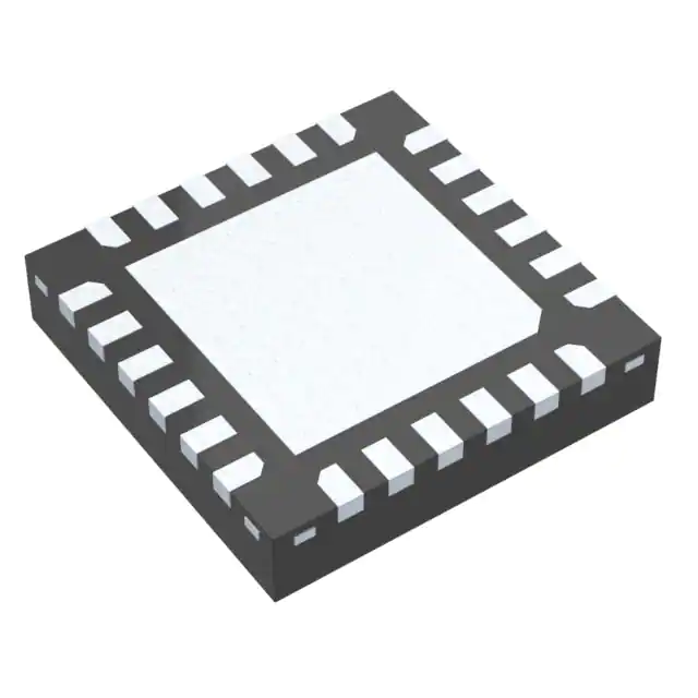
- Part No.:
- HMC980LP4E
- Manufacturer:
- Analog Devices Inc.
- Category:
- Power Management - Specialized
- Package:
- 24-VFQFN Exposed Pad
- Datasheet:
-
 HMC980LP4E.pdf
- Description:
- IC ACTIVE BIAS CONTROLLER 24QFN
- Quantity:
- Payment:

- Shipping:

Inventory:154
Please send an inquiry. Send us your inquiry, and we will respond immediately.
Product details
Overview
HMC980LP4E from Analog Devices is a high-current active bias controller IC designed to automatically regulate gate voltage for RF power amplifiers, supporting drain currents up to 1.6 A and drain supply voltages from 5 V to 16.5 V. It integrates an internal negative voltage generator (−2.46 V), dual gate control (VGATE and VG2), and over/undercurrent alarm with hysteresis - enabling stable Class A amplifier biasing in microwave radio, VSAT, and cellular base station applications.
For engineers reviewing the HMC980LP4E datasheet, HMC980LP4E pinout, HMC980LP4E application, or HMC980LP4E equivalent, key selection considerations include its 24-lead 4 mm × 4 mm LFCSP package, adjustable RDS_ON via S0/S1 logic inputs, ±4 mA VGATE sink/source capability, TRIGOUT daisy-chain signaling, and precise drain current set accuracy using external ISENSE resistor networks.
Technical Context
The HMC980LP4E implements a closed-loop analog feedback system that continuously adjusts VGATE to maintain constant IDRAIN despite supply, temperature, and process variations - eliminating factory calibration. Its internal MOSFET switch between VDD and VDRAIN enables safe power-up sequencing: VGATE is pulled to VNEG before VDRAIN is applied, ensuring the external amplifier remains fully pinched off during startup.
It features dual-domain operation: a high-voltage domain (VDD: 5–16.5 V) powers the output stage and RF amplifier supply path, while a low-voltage digital domain (VDIG: 3.3–5 V) powers logic, reference, and control circuitry. The integrated charge pump (300 kHz) generates VNEG for depletion-mode biasing, and VG2 provides a fixed secondary gate voltage adjustable via VG2_CONT resistor divider.
Key Specifications
| Parameter | Value and Actual Design Meaning |
|---|---|
| Drain Current Range | 0.05 A to 1.6 A - digitally selectable in four ranges via S0/S1 pins, enabling optimized RDS_ON (0.7–2.8 Ω) per load requirement |
| VDD Supply Range | 5 V to 16.5 V - supports wide-range RF amplifier drain supplies; absolute max 18 V |
| VNEG Output | −2.46 V - internally generated negative bias for depletion-mode FETs; 60 mA sourcing capability |
| VGATE Sink/Source | ±4 mA - actively drives gate capacitance across RF input power variations without external buffers |
| VDIG Supply | 3.3 V to 5 V - powers digital control logic; quiescent current 3.5 mA at 3.3 V |
| Operating Temp | −40°C to +85°C - specified performance across full industrial temperature range |
| Drain Current Stability | 0.023 %/°C - minimal drift ensures consistent RF gain and linearity without recalibration |
Pinout & Package
Package: 24-lead, 4 mm × 4 mm LFCSP (HCP-24-21), RoHS-compliant, with exposed thermal pad (EPAD) for enhanced heat dissipation (θJA = 49.4°C/W).
| Pin/Terminal | Circuit Role | Design Meaning |
|---|---|---|
| 1, 2 - VDD | High-voltage supply input | Primary power rail for internal MOSFET and amplifier drain path; must exceed VDRAIN by IDRAIN × RDS_ON |
| 3, 4 - S0, S1 | Digital configuration inputs | Select one of four RDS_ON settings (0.7–2.8 Ω) to match target drain current range |
| 5 - EN | Enable control input | Active-high (≥1.4 V) enables VGATE/VG2/VDRAIN; internal pull-up to VDIG allows default-on operation |
| 6 - ALM | Alarm status output | Active-high signal referenced to VDIG indicates overcurrent or undercurrent fault; no effect on bias loop operation |
| 9 - VDIG | Digital supply input | 3.3–5 V logic rail powering control circuitry; must be powered before VDD and VNEG |
| 10 - VREF | Internal reference output | Stable 1.44 V reference used to adjust VNEG and VGATE threshold voltages externally |
| 11 - VNEGFB | Negative voltage feedback | Floating enables internal VNEG generator; grounded disables it for external negative supply use |
| 12 - VGATEFB | VGATE threshold control | Floating configures for depletion-mode; grounded configures for enhancement-mode amplifier biasing |
| 13 - VG2_CONT | VG2 voltage setting input | Resistor-divider input to set VG2 level (1 V to VDD − 1.3 V); VG2 ≈ VG2_CONT − 1.3 V |
| 14 - VG2 | Secondary gate output | Fixed positive gate voltage for dual-gate amplifiers; not regulated by bias loop |
| 15 - VNEG | Negative supply input | Accepts internal CP_OUT or external negative source; must be powered after VDIG and before VDD |
| 16 - VGATE | Main gate control output | Regulated output driving amplifier gate; requires 2.2 µF local bypass capacitor for stability |
| 17, 18 - VDRAIN | Drain supply output | Switched VDD output applied to amplifier drain; decoupling ≥10 nF required at amplifier VDD pin |
| 19 - TRIGOUT | Daisy-chain trigger output | Active-high pulse when bias loop stabilizes; used to enable next HMC980LP4E in cascade |
| 20 - ISENSE | Drain current sense input | Connects to precision RSENSE (e.g., 0.5%, ±25 ppm) to set target IDRAIN via R = 150 / IDRAIN |
| 21, 22, 23 - ALML, ISET, ALMH | Alarm threshold inputs | Set ±6% (or asymmetric) over/undercurrent limits using precision resistors tied to ISET |
| 24 - FIXBIAS | Bias accuracy calibration | 10 kΩ precision resistor to ground ensures optimal bias accuracy and minimizes offset |
| EPAD | Thermal & electrical ground | Exposed pad must connect to low-impedance PCB ground plane for thermal management and noise reduction |
Key Features
| Feature | Design Value |
|---|---|
| Automatic gate voltage adjustment | Eliminates manual calibration by dynamically regulating VGATE to hold IDRAIN constant across temperature, supply, and process variation |
| Adjustable internal RDS_ON | Four discrete MOSFET on-resistance values (0.7–2.8 Ω) selected via S0/S1, minimizing conduction loss at each current range |
| Integrated negative voltage generator | On-chip 300 kHz charge pump delivers −2.46 V at up to 60 mA, enabling direct biasing of depletion-mode GaAs/GaN amplifiers |
| Safe power sequencing | Hardware-enforced startup order: VGATE pulled to VNEG → VDRAIN enabled → VG2 activated → VGATE ramped to target, preventing amplifier damage |
| Dual gate control (VGATE + VG2) | Simultaneous regulation of primary gate (VGATE, closed-loop) and secondary gate (VG2, open-loop fixed offset) for dual-gate RF amplifiers |
| TRIGOUT daisy-chain capability | Hardware-triggered output signals stabilization completion, enabling synchronized multi-amplifier biasing without external timing controllers |
Applications
| Microwave Radio Transceivers | VSAT Terminals |
|---|---|
Use Scenario: Biasing high-efficiency GaN power amplifiers in Ku-band transceivers requiring stable gain and EVM over temperature. IC Role / Device Role / Timing Role: Active bias controller maintaining constant IDRAIN during RF burst transmission and thermal cycling. Use Value: Enables >1.2 A drain current with <0.023%/°C drift, preserving adjacent channel power ratio (ACPR) without recalibration. |
Use Scenario: Providing dual-gate bias for low-noise, high-linearity MMIC amplifiers in portable satellite communication terminals. IC Role / Device Role / Timing Role: Simultaneous VGATE (regulated) and VG2 (fixed offset) generation for cascode amplifier configurations. Use Value: Eliminates need for two independent bias supplies; VG2 accuracy ±1.3 V offset ensures proper cascode DC operating point. |
| Cellular Base Station PA Modules | Fiber Optic Modulator Drivers |
Use Scenario: Biasing Doherty amplifier carrier and peaking stages in 5G massive MIMO active antenna units. IC Role / Device Role / Timing Role: Independent HMC980LP4E units per stage, coordinated via TRIGOUT daisy-chain for synchronized enable timing. Use Value: Ensures identical quiescent current matching (<±2%) between carrier/peaking paths, critical for Doherty efficiency optimization. |
Use Scenario: Biasing high-speed Mach-Zehnder modulator driver amplifiers requiring ultra-stable DC operating points for low-jitter optical transmission. IC Role / Device Role / Timing Role: Precision IDRAIN regulation (via 0.1% RSENSE) to maintain linear transfer function under varying laser temperature. Use Value: Achieves <0.02%/°C drain current stability, reducing optical eye diagram closure and bit error rate (BER) degradation. |
Equivalent & Alternatives
The following parts are listed as comparable options for similar active RF amplifier biasing applications.
| Alternative Part | Technical Difference | Application Difference | Selection Advice |
|---|---|---|---|
| LM3478MM/NOPB | Step-down DC/DC controller with external MOSFET; no integrated gate regulation, no VNEG, no TRIGOUT | Suitable only for basic drain supply switching - lacks closed-loop IDRAIN control and dual-gate support | Use only if biasing simple enhancement-mode devices without current stability requirements |
| MAX2034ETA+T | RF amplifier bias controller with 0.8 A max IDRAIN, no internal VNEG generator, 16-pin TQFN package | Limited to lower-current amplifiers; requires external negative supply for depletion-mode use | Select when drain current ≤800 mA and board space constraints favor smaller footprint |
Compared with LM3478MM/NOPB and MAX2034ETA+T, the HMC980LP4E uniquely combines 1.6 A closed-loop current regulation, integrated −2.46 V generation, dual-gate outputs, and hardware daisy-chain triggering - making it the only solution qualified for high-power, multi-stage, depletion-mode RF amplifier biasing in microwave infrastructure.
Availability
HMC980LP4E is available at Aetrix Electronics and suitable for microwave radio, VSAT terminal, and cellular base station applications requiring stable component supply, long-term lifecycle continuity, and traceable sourcing for RF power amplifier subsystems.
Supply support for HMC980LP4E includes scheduled delivery planning, volume procurement assistance, BOM continuity management, traceable sourcing, and lifecycle availability coordination for OEM customers, industrial embedded developers, connected-device designers, and electronics production programs.
Manufacturer
Analog Devices is a global leader in high-performance analog, mixed-signal, and RF ICs, serving communications, industrial, and aerospace markets with precision signal processing solutions.
The HMC980LP4E belongs to Analog Devices' Hittite Microwave product line, engineered specifically for high-reliability RF power amplifier biasing in microwave infrastructure - emphasizing thermal robustness, sequencing safety, and calibration-free operation.
FAQ
What is the maximum drain current supported by the HMC980LP4E?
The HMC980LP4E supports adjustable drain current up to 1.6 A, achieved when both S0 and S1 pins are driven to VDIG. This maximum is validated across the full operating temperature range (−40°C to +85°C) and requires appropriate PCB thermal design due to power dissipation. At 1.6 A, the internal MOSFET's RDS_ON is 0.7 Ω, resulting in ~1.12 W conduction loss - necessitating use of the exposed EPAD for thermal management.
How does the HMC980LP4E handle power-up sequencing for RF amplifiers?
The HMC980LP4E enforces strict hardware-based power-up sequencing: first pulling VGATE to VNEG to pinch off the amplifier, then enabling VDRAIN, followed by VG2 activation, and finally ramping VGATE to achieve target IDRAIN. This sequence prevents destructive current surges during startup. The TRIGOUT pin signals completion of this sequence, enabling cascaded devices to begin their own startup only after stabilization.
Can the HMC980LP4E bias both enhancement-mode and depletion-mode RF amplifiers?
Yes - the HMC980LP4E supports both amplifier types. For depletion-mode devices, VNEGFB is left floating to enable the internal −2.46 V generator, and VGATEFB is also left floating. For enhancement-mode devices, VNEGFB is grounded to disable the charge pump, and VGATEFB is shorted to ground to configure the threshold. This dual-mode flexibility is confirmed in the Functional Block Diagram and General Description sections of the Rev. C datasheet.
What is the role of the FIXBIAS pin on the HMC980LP4E?
The FIXBIAS pin requires connection of a precision 10 kΩ resistor (0.5% tolerance, ±25 ppm/°C TCR) to ground to ensure optimal bias accuracy and minimize offset errors in the current-sense amplifier. Omitting this resistor or using non-precision components degrades IDRAIN regulation accuracy beyond the specified 0.023%/°C drift, directly impacting RF amplifier linearity and gain stability.
Does the HMC980LP4E provide protection against short-circuit faults?
Yes - the HMC980LP4E includes self-protection circuitry that detects short circuits on VDRAIN or VNEG. Upon detection, it immediately disables VDRAIN and VGATE outputs and pulls VGATE to VNEG to safely shut down the amplifier. Recovery requires either a full power cycle or toggling the EN pin; the device remains latched in fault mode until reset, preventing automatic re-engagement into a hazardous condition.
HMC980LP4E Specifications
- Product attributes
- Attribute value
- Manufacturer:
- Analog Devices Inc.
- Series:
- -
- Package/Case:
- 24-VFQFN Exposed Pad
- Packaging:
- Strip
- Product Status:
- Active
- Applications:
- Current Biasing
- Current - Supply:
- 20mA
- Voltage - Supply:
- 5V ~ 16.5V
- Operating Temperature:
- -55°C ~ 85°C
- Grade:
- -
- Qualification:
- -
- Mounting Type:
- Surface Mount
- Supplier Device Package:
- 24-QFN (4x4)
HMC980LP4E FAQ
1.How can I place an order for HMC980LP4E through Aetrix?
Please submit a Request for Quotation (RFQ) for HMC980LP4E on Aetrix. Our sales agent will provide a competitive quotation and guide you through the order confirmation once you accept the terms.
2.Are the price and stock information for HMC980LP4E reliable?
The price and inventory of HMC980LP4E are updated periodically and may fluctuate due to market conditions. Stock and pricing data are typically refreshed every 24 hours. Quotation validity for HMC980LP4E is usually 5 days.
3.What payment methods are accepted for HMC980LP4E?
We accept Wire Transfer, PayPal, Credit Card, Western Union, MoneyGram, and Escrow for HMC980LP4E transactions.
Note: Certain payment methods may incur a processing fee.
4.How is shipping managed for HMC980LP4E?
HMC980LP4E orders can be shipped via leading logistics carriers, including DHL, UPS, FedEx, TNT, or Registered Mail.
Once your HMC980LP4E order is processed, you will receive an email with the shipment details and tracking number.
Note: Tracking information may take up to 24 hours to appear. Express delivery typically takes 3–5 business days.
5.How can I obtain technical support or documentation for HMC980LP4E?
For technical support, including HMC980LP4E datasheets, pinout diagrams, or application guidance, please contact our engineering support team. They can provide detailed documentation and assistance for your HMC980LP4E requirements.
6.How does Aetrix verify that HMC980LP4E is sourced from the original manufacturer or authorized distributors?
All HMC980LP4E products on Aetrix are procured from qualified distributors and authorized channels. Our dedicated quality assurance team conducts strict verification, including traceability checks and, if necessary, third-party testing. This ensures that HMC980LP4E meets industry standards.
7.What is the process for return or replacement of HMC980LP4E?
All HMC980LP4E units undergo pre-shipment inspection (PSI). If there is an issue with HMC980LP4E, returns or replacements are accepted under the following conditions:
1.Quantity discrepancies, incorrect items, or visible external defects (such as breakage or corrosion), acknowledged by Aetrix.
2.The issue is reported within 90 days of delivery.
3.The HMC980LP4E part is unused and in its original packaging.
Return procedure for HMC980LP4E:
1.Submit a request within 90 days.
2.Obtain a Return Material Authorization (RMA) from Aetrix.
HMC980LP4E Tags

-
TPS2511DGNR
Texas Instruments

-
UTC2000/MG
Microchip Technology

-
TUSB320HAIRWBR
Texas Instruments

-
TPS61252DSGR
Texas Instruments

-
PI5USB30216CXUAEX
Diodes Incorporated

-
SN6501DBVR
Texas Instruments

-
CYPD3177-24LQXQT
Infineon Technologies
-
SN6501QDBVRQ1
Texas Instruments

-
STUSB1600AQTR
STMicroelectronics

-
SN6505BDBVR
Texas Instruments
-
SN6501DBVT
Texas Instruments

-
TPS65150PWPR
Texas Instruments
Tech Hub

A practical engineering guide to 3.3V and 5V logic compatibility, input thresholds, resistor dividers, translator ICs, MOSFET level shifting, I2C pull-ups, timing limits and power-sequencing risks.

The 74HC595 uses push-pull logic outputs, while the TPIC6B595 uses 50 V open-drain DMOS sinks for higher-power loads. This guide compares timing, current limits, 3.3 V interfacing, load wiring, thermal…

The 74HC595 converts serial data into eight stable parallel outputs. This guide covers pin functions, shift and storage timing, OE and MR behavior, drive-current limits, cascading, voltage compatibilit…

A technical comparison of level-sensitive latches and edge-triggered flip-flops, covering timing windows, setup and hold limits, master–slave operation, time borrowing, race-through, HDL inference and…

A D latch stores one bit while Enable controls when data can pass. This reference covers gate-level operation, truth tables, transparency, setup and hold timing, LE versus OE, common ICs and practical …

An SR latch stores one bit through cross-coupled feedback. This engineering reference covers NOR and NAND implementations, truth tables, forbidden-state recovery, gated operation, switch debouncing, fa…

Latch circuits retain one bit through feedback. This technical reference covers SR and D latches, truth tables, transparency, timing limits, latch-versus-flip-flop behavior, applications and common log…

An engineering guide to LED driver operation, constant-current and constant-voltage outputs, linear and switching topologies, dimming, IC selection, calculations, replacement compatibility, and fault c…

Operational amplifier guide covering op amp basics, feedback, ideal vs real op amps, common configurations, buffer circuits, offset, bias current, gain-bandwidth, slew rate, rail-to-rail limits and sel…

Jumper cables guide covering safe connection order, red and black clamp placement, final ground connection, cable gauge, length, clamp quality, copper vs CCA cables, jump starter comparison and battery…


