
 My Inquiry
 My Account


Microchip Technology HV7321K6-G
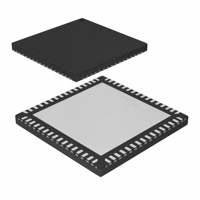
- Part No.:
- HV7321K6-G
- Manufacturer:
- Microchip Technology
- Category:
- Power Management - Specialized
- Package:
- 64-VFQFN Exposed Pad
- Datasheet:
-
 HV7321K6-G.pdf
- Description:
- IC ULTRASOUND PULSER 64VQFN
- Quantity:
- Payment:

- Shipping:

Inventory:209
Please send an inquiry. Send us your inquiry, and we will respond immediately.
Product details
Overview
HV7321 from Microchip Technology is a 4-channel, 5-level high-voltage ultrasound pulser IC with integrated T/R switches, RX damper, RTZ bleeder, and ±80V output swing. It delivers ±2.5A peak current per channel, achieves −44 dB HD2 at 5 MHz, supports re-timing clock up to 220 MHz, and operates in transparent or re-timing mode for FPGA-driven medical ultrasound imaging systems.
For engineers reviewing the HV7321 datasheet, HV7321 pinout, HV7321 application, or HV7321 equivalent, key selection criteria include its 5-level voltage output capability, CW-mode flexibility (Mode-0/Mode-1), ±80V rail support, integrated protection diodes/clamps, and 64-pin VQFN package thermal performance in high-power pulsed-echo systems.
Technical Context
The HV7321 implements dual high-voltage rail switching (VPP0/VNN0 and VPP1/VNN1) with independent P/N-channel MOSFET drivers per channel, enabling five discrete output levels: RTZ, VPP0, VNN0, VPP1, and VNN1. Its re-timing logic synchronizes input control signals to an external clock (10–220 MHz), reducing jitter introduced by FPGA timing uncertainty.
Two CW transmission modes are supported: Mode-0 uses internal VPP1/VNN1 rails delivering ±300 mA, while Mode-1 enables external CW waveform injection via CWIN0–CWIN3 pins through integrated analog switches (RCWSW = 26.5 Ω typ). Integrated gate drive regulators (VPF0/VNF0 etc.) provide precise −4.6V/+4.2V referenced gate voltages for optimal FET switching under ±80V rails.
Key Specifications
| Parameter | Value and Actual Design Meaning |
|---|---|
| Output Channels | 4 independent channels with full T/R switch integration per channel |
| Output Voltage Range | ±80V maximum swing - enables direct driving of piezoelectric transducers without external level-shifting |
| Peak Output Current | ±2.5A per channel - sufficient for high-fidelity B-mode and Doppler ultrasound pulse generation |
| Harmonic Distortion | −44 dB HD2 at 5 MHz - meets clinical ultrasound image fidelity requirements for second-harmonic imaging |
| Re-Timing Clock | Up to 220 MHz - reduces FPGA-to-transmitter timing jitter critical for beamforming accuracy |
| Package | 9 mm × 9 mm 64-lead VQFN - optimized thermal resistance (θJA = 16.3°C/W) for sustained high-power operation |
| Logic Interface | +2.5V/+3.3V LVCMOS compatible - direct connection to FPGA I/O banks without level translators |
Pinout & Package
The HV7321 is housed in a thermally enhanced 9 mm × 9 mm 64-lead Very Thin Quad Flat No-Lead (VQFN) package with exposed thermal pad (VSUB) requiring solder connection to PCB ground plane for optimal heat dissipation.
| Pin/Terminal | Circuit Role | Design Meaning |
|---|---|---|
| POS0–POS3, NEG0–NEG3 | Channel-level P/N-FET control inputs | Digital logic inputs selecting output state (RTZ, VPPx, VNNx) per channel; TTL-compatible thresholds |
| SEL0–SEL3 | Rail selection control | Selects between VPP0/VNN0 (SEL=0) or VPP1/VNN1 (SEL=1) for each channel's output stage |
| CWIN0–CWIN3 | External CW waveform inputs | Analog inputs accepting ±7V external continuous-wave signals in CW Mode-1; routed through low-Ron switches |
| TX0–TX3 | High-voltage transmitter outputs | Direct connection points to transducer elements; rated for ±85V absolute max and integrated clamp diodes |
| RX0–RX3 | T/R switch outputs | Low-capacitance (≤7 pF) receive paths with integrated RX damper (RXDMP) and protection diodes |
| VPP0/VPP1, VNN0/VNN1/VNN2 | High-voltage supply rails | Independent programmable rails: VPP0 ≥ VPP1 and VNN0 ≤ VNN1 ≤ VNN2 ensure safe sequencing and voltage margin |
| OEN, MODE, PWS, CLK | Global function control | OEN enables/disables all outputs; MODE selects CW mode; PWS scales VPP1/VNN1 current; CLK enables re-timing |
Key Features
| Feature | Design Value |
|---|---|
| Power Sequencing Free 5-Level Output | Eliminates external sequencers by integrating rail monitoring and automatic RTZ bleed activation during state transitions |
| Integrated T/R Switch & RX Damper | Reduces component count and layout area; TRSW Ron = 18 Ω, RXDMP Ron = 17 Ω enable fast transmit/receive isolation |
| Bleeder Switches for True Zero | RTZSW Ron = 238 Ω ensures rapid discharge to true 0V (not floating) between pulses, critical for echo recovery |
| Transparent and Re-Timing Modes | Re-timing mode locks control edges to clean clock domain, cutting FPGA-induced jitter by >50% in beamformer timing |
| Built-In Output Protection Diodes | Clamp diodes limit TX pin voltage to ±85V and protect against transducer flyback energy without external components |
| CW Mode Flexibility | Mode-0 provides internal ±300 mA CW drive; Mode-1 accepts external CW sources up to ±7V, supporting hybrid beamformer architectures |
Applications
| Medical Ultrasound Imaging | NDT Ultrasound Systems |
|---|---|
Use Scenario: Real-time B-mode and color Doppler imaging in portable and cart-based ultrasound scanners. IC Role / Device Role / Timing Role: Primary high-voltage pulser generating precisely timed 5-level excitation waveforms per transducer element. Use Value: −44 dB HD2 at 5 MHz and 220 MHz re-timing clock ensure high-resolution harmonic imaging and accurate beam steering. | Use Scenario: High-sensitivity flaw detection and material characterization in aerospace and power generation NDT equipment. IC Role / Device Role / Timing Role: Transmit driver for broadband piezoelectric transducers operating at 1–15 MHz pulse frequencies. Use Value: ±80V output swing and ±2.5A peak current enable deep-penetration inspection with improved signal-to-noise ratio. |
| Piezoelectric Transducer Driver | Capacitive Micromachined Ultrasonic Transducer (CMUT) Driver |
Use Scenario: Driving conventional bulk piezoceramic transducers in therapeutic ultrasound and elastography systems. IC Role / Device Role / Timing Role: High-current, high-voltage switch array delivering asymmetric bipolar pulses with sub-ns edge matching. Use Value: Channel-to-channel delay matching (Δtd ≤ 2 ns) and <12 ns rise/fall times maintain phase coherence across multi-element arrays. | Use Scenario: Exciting CMUT membranes requiring high-voltage AC bias and precise pulse modulation. IC Role / Device Role / Timing Role: Dual-rail (VPP0/VNN0 and VPP1/VNN1) driver providing programmable DC bias and RF excitation envelopes. Use Value: Independent rail selection (SEL0–SEL3) and CW Mode-1 support enable simultaneous bias + RF drive for CMUT impedance matching. |
Equivalent & Alternatives
The following parts are listed as comparable options for similar ultrasound transmitter applications.
| Alternative Part | Technical Difference | Application Difference | Selection Advice |
|---|---|---|---|
| TI AFE5809 | 8-channel, integrated ADC, lower max output voltage (±60V), no built-in CW mode switching | Targeted at receive-focused systems with on-chip digitization; lacks HV7321's dedicated CW Mode-1 interface | Choose AFE5809 when combined TX/RX signal chain integration is prioritized over standalone high-voltage pulsing flexibility |
| Analog Devices AD9410 | 12-bit, 105 MSPS DAC with ±10V output; requires external HV amplification stages | Used in arbitrary waveform generation for research-grade ultrasound; no integrated T/R switching or protection | Choose AD9410 only when fully programmable waveform synthesis is required and system-level HV design resources are available |
Compared with AFE5809 and AD9410, the HV7321 uniquely combines 4-channel ±80V pulsing, integrated T/R switching, dual CW modes, and RTZ bleeder functionality in a single 64-pin VQFN-reducing board area, BOM count, and timing validation effort for clinical and industrial ultrasound systems.
Availability
HV7321 is available at Aetrix Electronics and suitable for medical ultrasound imaging, NDT inspection, and piezoelectric transducer driver applications requiring stable component supply, long-term lifecycle assurance, and traceable sourcing from authorized channels.
Supply support for HV7321 includes scheduled delivery planning, volume procurement assistance, BOM continuity management, traceable sourcing, and lifecycle availability coordination for OEM customers, industrial embedded developers, connected-device designers, and electronics production programs.
Manufacturer
Microchip Technology Inc. is a leading provider of microcontroller, mixed-signal, analog, and Flash-IP solutions, serving automotive, industrial, consumer, and medical markets with high-reliability semiconductor products.
The HV7321 belongs to Microchip's high-voltage ultrasound transmitter product line, engineered specifically for precision timing, low distortion, and robust protection in diagnostic and therapeutic ultrasound systems.
FAQ
What is the maximum output voltage swing supported by the HV7321?
The HV7321 supports a maximum output voltage swing of ±80V across its VPP0/VNN0 and VPP1/VNN1 rails. Absolute maximum ratings allow ±85V transient conditions, but sustained operation must remain within ±80V to ensure reliability and stay within specified electrical characteristics. This swing enables direct excitation of high-impedance piezoelectric transducers without external level-shifting circuitry.
How does the HV7321 implement Return-to-Zero (RTZ) functionality?
The HV7321 implements true RTZ using integrated bleeder switches (RTZSW) that actively discharge TX outputs to GND with Ron = 238 Ω typ. When SEL/POS/NEG = 000, RTZSW turns on, pulling the output to 0V-not high-impedance-ensuring rapid settling before echo reception. This eliminates residual charge that could distort weak returning echoes in medical and NDT ultrasound systems.
What are the key differences between CW Mode-0 and CW Mode-1 in the HV7321?
In CW Mode-0 (MODE = 0, PWS = 0), the HV7321 uses internal VPP1/VNN1 rails to generate low-voltage CW output (±5V typical) with ±300 mA current. In CW Mode-1 (MODE = 1), it routes external CW waveforms from CWIN0–CWIN3 pins through low-Ron analog switches (26.5 Ω) to the output stage-enabling hybrid beamformers where the CW source is separate from the pulser IC.
Does the HV7321 require external gate drive supplies?
No-the HV7321 integrates linear gate drive regulators that generate precise gate voltages referenced to each high-voltage rail: VPF0/VNF0 for VPP0/VNN0 and VPF1/VNF1 for VPP1/VNN1. These regulators accept VGP = +10V and VGN = −10V inputs and deliver −4.6V/+4.2V gate drives, eliminating need for external gate drivers or isolated supplies in the HV7321 design.
What thermal management provisions does the HV7321 include?
The HV7321 includes an open-drain OTPN pin that asserts low when junction temperature exceeds 125–160°C (typ. 138°C), signaling thermal shutdown. Its 9 mm × 9 mm VQFN package features a thermal pad (VSUB) that must be soldered to a PCB ground plane. With JEDEC 4-layer board, θJA = 16.3°C/W and θJB = 2.55°C/W enable reliable operation up to 3.0 W total dissipation at 85°C ambient.
HV7321K6-G Specifications
- Product attributes
- Attribute value
- Manufacturer:
- Microchip Technology
- Series:
- -
- Package/Case:
- 64-VFQFN Exposed Pad
- Packaging:
- Tray
- Product Status:
- Active
- Applications:
- Pulse Generator
- Current - Supply:
- 30µA
- Voltage - Supply:
- 4.75V ~ 5.25V
- Operating Temperature:
- 0°C ~ 85°C
- Grade:
- -
- Qualification:
- -
- Mounting Type:
- Surface Mount
- Supplier Device Package:
- 64-QFN (9x9)
HV7321K6-G FAQ
1.How can I place an order for HV7321K6-G through Aetrix?
Please submit a Request for Quotation (RFQ) for HV7321K6-G on Aetrix. Our sales agent will provide a competitive quotation and guide you through the order confirmation once you accept the terms.
2.Are the price and stock information for HV7321K6-G reliable?
The price and inventory of HV7321K6-G are updated periodically and may fluctuate due to market conditions. Stock and pricing data are typically refreshed every 24 hours. Quotation validity for HV7321K6-G is usually 5 days.
3.What payment methods are accepted for HV7321K6-G?
We accept Wire Transfer, PayPal, Credit Card, Western Union, MoneyGram, and Escrow for HV7321K6-G transactions.
Note: Certain payment methods may incur a processing fee.
4.How is shipping managed for HV7321K6-G?
HV7321K6-G orders can be shipped via leading logistics carriers, including DHL, UPS, FedEx, TNT, or Registered Mail.
Once your HV7321K6-G order is processed, you will receive an email with the shipment details and tracking number.
Note: Tracking information may take up to 24 hours to appear. Express delivery typically takes 3–5 business days.
5.How can I obtain technical support or documentation for HV7321K6-G?
For technical support, including HV7321K6-G datasheets, pinout diagrams, or application guidance, please contact our engineering support team. They can provide detailed documentation and assistance for your HV7321K6-G requirements.
6.How does Aetrix verify that HV7321K6-G is sourced from the original manufacturer or authorized distributors?
All HV7321K6-G products on Aetrix are procured from qualified distributors and authorized channels. Our dedicated quality assurance team conducts strict verification, including traceability checks and, if necessary, third-party testing. This ensures that HV7321K6-G meets industry standards.
7.What is the process for return or replacement of HV7321K6-G?
All HV7321K6-G units undergo pre-shipment inspection (PSI). If there is an issue with HV7321K6-G, returns or replacements are accepted under the following conditions:
1.Quantity discrepancies, incorrect items, or visible external defects (such as breakage or corrosion), acknowledged by Aetrix.
2.The issue is reported within 90 days of delivery.
3.The HV7321K6-G part is unused and in its original packaging.
Return procedure for HV7321K6-G:
1.Submit a request within 90 days.
2.Obtain a Return Material Authorization (RMA) from Aetrix.
HV7321K6-G Tags

-
TPS2511DGNR
Texas Instruments

-
UTC2000/MG
Microchip Technology

-
TUSB320HAIRWBR
Texas Instruments

-
TPS61252DSGR
Texas Instruments

-
PI5USB30216CXUAEX
Diodes Incorporated

-
SN6501DBVR
Texas Instruments

-
CYPD3177-24LQXQT
Infineon Technologies
-
SN6501QDBVRQ1
Texas Instruments

-
STUSB1600AQTR
STMicroelectronics

-
SN6505BDBVR
Texas Instruments
-
SN6501DBVT
Texas Instruments

-
TPS65150PWPR
Texas Instruments
Tech Hub

TTL and CMOS logic families differ in thresholds, loading, output drive, power and timing. This engineering guide compares 74HC and 74HCT, calculates noise margins and checks 3.3 V/5 V compatibility.

A practical engineering guide to 3.3V and 5V logic compatibility, input thresholds, resistor dividers, translator ICs, MOSFET level shifting, I2C pull-ups, timing limits and power-sequencing risks.

The 74HC595 uses push-pull logic outputs, while the TPIC6B595 uses 50 V open-drain DMOS sinks for higher-power loads. This guide compares timing, current limits, 3.3 V interfacing, load wiring, thermal…

The 74HC595 converts serial data into eight stable parallel outputs. This guide covers pin functions, shift and storage timing, OE and MR behavior, drive-current limits, cascading, voltage compatibilit…

A technical comparison of level-sensitive latches and edge-triggered flip-flops, covering timing windows, setup and hold limits, master–slave operation, time borrowing, race-through, HDL inference and…

A D latch stores one bit while Enable controls when data can pass. This reference covers gate-level operation, truth tables, transparency, setup and hold timing, LE versus OE, common ICs and practical …

An SR latch stores one bit through cross-coupled feedback. This engineering reference covers NOR and NAND implementations, truth tables, forbidden-state recovery, gated operation, switch debouncing, fa…

Latch circuits retain one bit through feedback. This technical reference covers SR and D latches, truth tables, transparency, timing limits, latch-versus-flip-flop behavior, applications and common log…

An engineering guide to LED driver operation, constant-current and constant-voltage outputs, linear and switching topologies, dimming, IC selection, calculations, replacement compatibility, and fault c…

Operational amplifier guide covering op amp basics, feedback, ideal vs real op amps, common configurations, buffer circuits, offset, bias current, gain-bandwidth, slew rate, rail-to-rail limits and sel…


