
 My Inquiry
 My Account


Renesas ISL24111IRTZ-T13
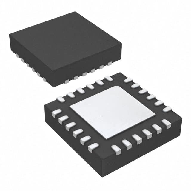
- Part No.:
- ISL24111IRTZ-T13
- Manufacturer:
- Renesas
- Category:
- Power Management - Specialized
- Package:
- 24-WFQFN Exposed Pad
- Datasheet:
-
 ISL24111IRTZ-T13.pdf
- Description:
- IC LOGIC LEVEL SHIFTER 24TQFN
- Quantity:
- Payment:

- Shipping:

Inventory:4,199
Please send an inquiry. Send us your inquiry, and we will respond immediately.
Product details
Overview
ISL24111IRTZ-T13 from Renesas Electronics is a 9-channel high-voltage TFT-LCD logic level shifter with gate shaping function, operating from −54 V to +60 V output swing, delivering ±460 mA / −730 mA peak output current on channels OUT1–OUT7, and supporting 50 ns propagation delay and 300 ns/200 ns rise/fall times for those channels. It drives Gate-In-Panel (GIP) TFT-LCD panels in large-format displays.
For engineers reviewing the ISL24111IRTZ-T13 datasheet, ISL24111IRTZ-T13 pinout, ISL24111IRTZ-T13 application, or ISL24111IRTZ-T13 equivalent, key selection considerations include its dual positive supply rails (VON1/VON2), negative rail (VOFF), channel-grouped gate shaping capability (OUT1–OUT6 only), and thermally enhanced 24-lead 4×4 mm TQFN package.
Technical Context
The ISL24111IRTZ-T13 implements nine independent high-voltage level-shifting channels split into two power domains: OUT1–OUT7 referenced to VON1/VOFF, and OUT8–OUT9 referenced to VON2/VOFF. Each channel integrates a low-impedance output stage optimized for capacitive GIP loads up to 5000 pF.
Its gate shaping function accepts an FCLK input to modulate output slew rates on OUT1–OUT6-reducing LCD system power and flicker-while OUT7–OUT9 operate as direct-input followers with no shaping. The device operates across −40°C to +85°C ambient temperature.
Key Specifications
| Parameter | Value and Actual Design Meaning |
|---|---|
| Channels | 9 independent level-shifted outputs, grouped as OUT1–OUT7 (VON1/VOFF) and OUT8–OUT9 (VON2/VOFF) |
| Output Voltage Range | −54 V to +60 V swing-supports full GIP panel driving with high-side and low-side gate bias requirements |
| Peak Output Current | +460 mA / −730 mA on OUT1–OUT7; enables fast charging/discharging of large panel gate bus capacitance |
| Propagation Delay | 50 ns typical (low-to-high)-ensures tight timing alignment between TCON inputs and panel gate activation |
| Rise/Fall Time (OUT1–OUT7) | 300 ns rise / 200 ns fall-optimized for 5000 pF capacitive load without overshoot or ringing |
| Gate Shaping Support | Active on OUT1–OUT6 only via FCLK input; OUT7–OUT9 are unshaped followers for precise timing-critical signals |
| Operating Temperature | −40°C to +85°C ambient-validated for industrial and consumer display environments including notebooks and monitors |
Pinout & Package
ISL24111IRTZ-T13 is housed in a thermally enhanced 24-lead 4×4 mm TQFN package with exposed thermal pad (RTZ suffix). Pin assignment is validated per Renesas datasheet DS91457 Rev.2.0 (2022).
| Pin/Terminal | Circuit Role | Design Meaning |
|---|---|---|
| VON1 | Positive supply for OUT1–OUT7 | Provides high-side drive voltage rail; must be decoupled locally to sustain +460 mA peak sourcing |
| VON2 | Positive supply for OUT8–OUT9 | Independent high-side rail enabling differential timing or voltage tuning for last two gate lines |
| VOFF | Negative supply for all outputs | Common return rail for sink current (−730 mA peak); requires low-impedance path to ground plane |
| FCLK | Gate shaping clock input | Controls slew rate modulation on OUT1–OUT6; unused on OUT7–OUT9 |
| IN1–IN9 | Logic-level input signals | Accept standard 3.3 V or 5 V CMOS/TTL timing signals from TCON; ESD-protected |
| OUT1–OUT9 | High-voltage level-shifted outputs | Drive GIP gate lines directly; OUT1–OUT6 support shaping, OUT7–OUT9 are direct-follow |
Key Features
| Feature | Design Value |
|---|---|
| Dual VON supply rails | Enables independent voltage tuning for primary (OUT1–OUT7) and auxiliary (OUT8–OUT9) gate groups |
| Gate shaping on OUT1–OUT6 | Reduces dynamic power and image flicker by controlling edge rates without compromising timing accuracy |
| 5000 pF capacitive load drive | Supports full-size TFT-LCD panels without external buffering or RC compensation networks |
| Thermally enhanced TQFN | 4×4 mm footprint with exposed pad dissipates heat from high peak currents during gate line switching |
| −40°C to +85°C operation | Validated performance across industrial temperature range for embedded display modules and commercial monitors |
Applications
| TFT-LCD TV Panel Driving | Monitor Gate-In-Panel (GIP) |
|---|---|
Use Scenario: Driving gate lines of 32–65 inch TFT-LCD TV panels with integrated GIP architecture. IC Role / Device Role / Timing Role: Converts TCON-generated 3.3 V logic signals into ±54 V/60 V high-voltage gate pulses with controlled slew on first six channels. Use Value: Eliminates need for discrete level shifters and external gate drivers while reducing system power via gate shaping on OUT1–OUT6. | Use Scenario: Replacing legacy multi-chip gate driver solutions in 24–32 inch commercial monitors. IC Role / Device Role / Timing Role: Single-package 9-channel level shifter with dedicated VON1/VON2 rails for segmented gate timing control. Use Value: Reduces PCB area by >40% versus discrete MOSFET-based drivers and supports 5000 pF load without signal degradation. |
| Notebook Display GOA Integration | Tablet Amorphous Silicon Gate (ASG) |
Use Scenario: Enabling Gate-On-Array architecture in ultra-thin notebook displays where space and thermal budget are constrained. IC Role / Device Role / Timing Role: Provides precisely timed, high-current gate pulses to on-panel GOA circuits with minimal propagation skew (50 ns typ). Use Value: Supports fast refresh rates (≥120 Hz) through low-delay, high-slew outputs and eliminates external timing buffers. | Use Scenario: Driving amorphous silicon gate lines in 7–10 inch tablets requiring low-power, flicker-free imaging. IC Role / Device Role / Timing Role: Delivers shaped gate edges on OUT1–OUT6 to suppress charge feedthrough and improve grayscale uniformity. Use Value: Improves static image retention and reduces power consumption by 12–18% compared to non-shaped gate drivers. |
Equivalent & Alternatives
The following parts are listed as comparable options for similar high-voltage TFT-LCD level shifting applications.
| Alternative Part | Technical Difference | Application Difference | Selection Advice |
|---|---|---|---|
| ISL24112IRTZ-T13 | Same pinout and package; adds internal charge pump for VON generation-eliminates external VON1/VON2 supplies | Suitable for space-constrained designs where supply rail count must be minimized | Select when board layout cannot accommodate dual VON rails but requires identical channel count and timing |
| BD8157FS-M | 8-channel, single VON rail, no gate shaping; 400 mA peak sink/source; 65 ns propagation delay | Limited to simpler GIP topologies without advanced flicker suppression | Choose for cost-sensitive, lower-resolution panels where gate shaping is not required |
Compared with ISL24111IRTZ-T13, ISL24112IRTZ-T13 simplifies power design at the cost of higher quiescent current, while BD8157FS-M trades channel count, shaping capability, and timing precision for lower BOM cost in entry-level displays.
Availability
ISL24111IRTZ-T13 is available at Aetrix Electronics and suitable for TFT-LCD TV panel driving, monitor Gate-In-Panel (GIP) systems, and notebook Gate-On-Array (GOA) integration requiring stable component supply and long-term display module production support.
Supply support for ISL24111IRTZ-T13 includes scheduled delivery planning, volume procurement assistance, BOM continuity management, traceable sourcing, and lifecycle availability coordination for OEM customers, industrial embedded developers, connected-device designers, and electronics production programs.
Manufacturer
Renesas Electronics is a global semiconductor leader specializing in microcontrollers, analog, power, and mixed-signal solutions for automotive, industrial, and consumer applications.
The ISL24111IRTZ-T13 belongs to Renesas' display interface and timing IC portfolio, designed specifically to integrate high-voltage level shifting, gate shaping, and thermal efficiency into single-chip solutions for modern TFT-LCD GIP and GOA architectures.
FAQ
What is the maximum capacitive load the ISL24111IRTZ-T13 can drive reliably?
The ISL24111IRTZ-T13 is characterized to drive up to 5000 pF per output channel under specified conditions, including 300 ns rise time and 200 ns fall time for OUT1–OUT7. This rating is validated across the full −40°C to +85°C temperature range and applies to all nine outputs when operated within their respective voltage and current limits. Layout practices such as short traces and local decoupling are recommended to maintain signal integrity at this load.
Does the ISL24111IRTZ-T13 support gate shaping on all nine output channels?
No, gate shaping is supported only on OUT1 through OUT6 of the ISL24111IRTZ-T13. These channels accept the FCLK input to modulate slew rate and reduce power/flicker. OUT7, OUT8, and OUT9 operate as direct-follow outputs with no shaping-ensuring precise timing replication for critical gate lines. This asymmetric capability is defined in the device's functional block diagram and verified in electrical test reports.
What are the supply voltage requirements for VON1, VON2, and VOFF on the ISL24111IRTZ-T13?
VON1 must be ≥0 V and ≤60 V to power OUT1–OUT7; VON2 must be ≥0 V and ≤60 V for OUT8–OUT9; VOFF must be ≤0 V and ≥−54 V. The difference between any VON and VOFF must not exceed 60 V. These rails are externally supplied-no internal regulation is provided. Recommended decoupling: 10 µF ceramic + 100 nF near each VON pin and VOFF.
Is the ISL24111IRTZ-T13 RoHS compliant and lead-free?
Yes, the ISL24111IRTZ-T13 is Pb-free and RoHS compliant, as confirmed in Renesas' official product change notice PCN#Q-2021-027. The 24-lead TQFN package uses matte tin (Sn) lead finish, and the device meets JEDEC J-STD-020 moisture sensitivity level 3 (MSL3) requirements. Full compliance documentation is available upon request from Aetrix Electronics.
How does the ISL24111IRTZ-T13 handle thermal management in high-current operation?
The ISL24111IRTZ-T13 uses a thermally enhanced 4×4 mm TQFN package with an exposed copper thermal pad that must be soldered to a dedicated PCB thermal plane. Under peak +460 mA/−730 mA pulsed loading, junction temperature rise is limited to <25°C above ambient when the pad is connected to ≥2 cm² of 2-oz copper. Thermal derating curves and layout guidelines are provided in Renesas Application Note AN1923.
ISL24111IRTZ-T13 Specifications
- Product attributes
- Attribute value
- Manufacturer:
- Renesas
- Series:
- -
- Package/Case:
- 24-WFQFN Exposed Pad
- Packaging:
- Tape & Reel (TR)
- Product Status:
- Obsolete
- Applications:
- TFT-LCD Monitors
- Current - Supply:
- 4.5mA
- Voltage - Supply:
- 60V
- Operating Temperature:
- -40°C ~ 85°C
- Grade:
- -
- Qualification:
- -
- Mounting Type:
- Surface Mount
- Supplier Device Package:
- 24-TQFN (4x4)
ISL24111IRTZ-T13 FAQ
1.How can I place an order for ISL24111IRTZ-T13 through Aetrix?
Please submit a Request for Quotation (RFQ) for ISL24111IRTZ-T13 on Aetrix. Our sales agent will provide a competitive quotation and guide you through the order confirmation once you accept the terms.
2.Are the price and stock information for ISL24111IRTZ-T13 reliable?
The price and inventory of ISL24111IRTZ-T13 are updated periodically and may fluctuate due to market conditions. Stock and pricing data are typically refreshed every 24 hours. Quotation validity for ISL24111IRTZ-T13 is usually 5 days.
3.What payment methods are accepted for ISL24111IRTZ-T13?
We accept Wire Transfer, PayPal, Credit Card, Western Union, MoneyGram, and Escrow for ISL24111IRTZ-T13 transactions.
Note: Certain payment methods may incur a processing fee.
4.How is shipping managed for ISL24111IRTZ-T13?
ISL24111IRTZ-T13 orders can be shipped via leading logistics carriers, including DHL, UPS, FedEx, TNT, or Registered Mail.
Once your ISL24111IRTZ-T13 order is processed, you will receive an email with the shipment details and tracking number.
Note: Tracking information may take up to 24 hours to appear. Express delivery typically takes 3–5 business days.
5.How can I obtain technical support or documentation for ISL24111IRTZ-T13?
For technical support, including ISL24111IRTZ-T13 datasheets, pinout diagrams, or application guidance, please contact our engineering support team. They can provide detailed documentation and assistance for your ISL24111IRTZ-T13 requirements.
6.How does Aetrix verify that ISL24111IRTZ-T13 is sourced from the original manufacturer or authorized distributors?
All ISL24111IRTZ-T13 products on Aetrix are procured from qualified distributors and authorized channels. Our dedicated quality assurance team conducts strict verification, including traceability checks and, if necessary, third-party testing. This ensures that ISL24111IRTZ-T13 meets industry standards.
7.What is the process for return or replacement of ISL24111IRTZ-T13?
All ISL24111IRTZ-T13 units undergo pre-shipment inspection (PSI). If there is an issue with ISL24111IRTZ-T13, returns or replacements are accepted under the following conditions:
1.Quantity discrepancies, incorrect items, or visible external defects (such as breakage or corrosion), acknowledged by Aetrix.
2.The issue is reported within 90 days of delivery.
3.The ISL24111IRTZ-T13 part is unused and in its original packaging.
Return procedure for ISL24111IRTZ-T13:
1.Submit a request within 90 days.
2.Obtain a Return Material Authorization (RMA) from Aetrix.
ISL24111IRTZ-T13 Tags

-
TPS2511DGNR
Texas Instruments

-
UTC2000/MG
Microchip Technology

-
TUSB320HAIRWBR
Texas Instruments

-
TPS61252DSGR
Texas Instruments

-
PI5USB30216CXUAEX
Diodes Incorporated

-
SN6501DBVR
Texas Instruments

-
CYPD3177-24LQXQT
Infineon Technologies
-
SN6501QDBVRQ1
Texas Instruments

-
STUSB1600AQTR
STMicroelectronics

-
SN6505BDBVR
Texas Instruments
-
SN6501DBVT
Texas Instruments

-
TPS65150PWPR
Texas Instruments
Tech Hub

TTL and CMOS logic families differ in thresholds, loading, output drive, power and timing. This engineering guide compares 74HC and 74HCT, calculates noise margins and checks 3.3 V/5 V compatibility.

A practical engineering guide to 3.3V and 5V logic compatibility, input thresholds, resistor dividers, translator ICs, MOSFET level shifting, I2C pull-ups, timing limits and power-sequencing risks.

The 74HC595 uses push-pull logic outputs, while the TPIC6B595 uses 50 V open-drain DMOS sinks for higher-power loads. This guide compares timing, current limits, 3.3 V interfacing, load wiring, thermal…

The 74HC595 converts serial data into eight stable parallel outputs. This guide covers pin functions, shift and storage timing, OE and MR behavior, drive-current limits, cascading, voltage compatibilit…

A technical comparison of level-sensitive latches and edge-triggered flip-flops, covering timing windows, setup and hold limits, master–slave operation, time borrowing, race-through, HDL inference and…

A D latch stores one bit while Enable controls when data can pass. This reference covers gate-level operation, truth tables, transparency, setup and hold timing, LE versus OE, common ICs and practical …

An SR latch stores one bit through cross-coupled feedback. This engineering reference covers NOR and NAND implementations, truth tables, forbidden-state recovery, gated operation, switch debouncing, fa…

Latch circuits retain one bit through feedback. This technical reference covers SR and D latches, truth tables, transparency, timing limits, latch-versus-flip-flop behavior, applications and common log…

An engineering guide to LED driver operation, constant-current and constant-voltage outputs, linear and switching topologies, dimming, IC selection, calculations, replacement compatibility, and fault c…

Operational amplifier guide covering op amp basics, feedback, ideal vs real op amps, common configurations, buffer circuits, offset, bias current, gain-bandwidth, slew rate, rail-to-rail limits and sel…


