
 My Inquiry
 My Account


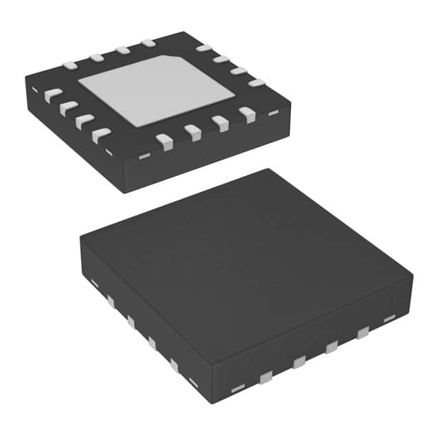
Renesas ISL6614CRZ
- Part No.:
- ISL6614CRZ
- Manufacturer:
- Renesas
- Category:
- Gate Drivers
- Package:
- 16-VQFN Exposed Pad
- Datasheet:
-
 ISL6614CRZ.pdf
- Description:
- IC GATE DRVR HALF-BRIDGE 16QFN
- Quantity:
- Payment:

- Shipping:

Inventory:2,043
Please send an inquiry. Send us your inquiry, and we will respond immediately.
Product details
Overview
ISL6614CRZ from Intersil is a dual advanced synchronous rectified buck MOSFET driver IC designed for two-phase interleaved core-voltage regulators driving N-channel high-side and low-side power MOSFETs. It delivers 3A sinking current, supports up to 1MHz switching frequency, features adaptive zero shoot-through protection, pre-POR overvoltage protection, and operates with 5V–12V gate drive voltage (PVCC) for efficiency optimization in microprocessor VRMs.
For engineers reviewing the ISL6614CRZ datasheet, ISL6614CRZ pinout, ISL6614CRZ application, or ISL6614CRZ equivalent, key selection considerations include its 16-lead QFN package with exposed thermal pad, three-state PWM input for controlled shutdown, integrated bootstrap Schottky diodes, and over-temperature protection with +42°C hysteresis - all critical for high-current, high-frequency DC/DC converter design.
Technical Context
The ISL6614CRZ integrates two independent gate drivers per channel, each controlling one high-side and one low-side N-MOSFET in a synchronous buck half-bridge. Its adaptive shoot-through protection monitors PHASE node voltage and body-diode conduction to dynamically adjust deadtime, minimizing freewheeling loss while preventing simultaneous conduction.
It implements Pre-POR overvoltage protection by connecting LGATE to PHASE before VCC reaches its 9.8V turn-on threshold, limiting output voltage via the low-side MOSFET's threshold during startup faults. The three-state PWM input provides a 1.8V–2.4V shutdown window with 245ns hold-off time to eliminate negative transients during power-down.
Key Specifications
| Parameter | Value and Actual Design Meaning |
|---|---|
| VCC Supply Voltage | 12V ±10% - powers internal analog circuitry; POR rising threshold at 9.8V typical ensures safe enablement after bias stabilization. |
| PVCC Drive Voltage Range | 5V to 12V ±10% - sets both upper and lower gate drive rails simultaneously, enabling trade-off optimization between gate charge loss and conduction loss. |
| Switching Frequency Support | Up to 1MHz - enables compact magnetics and high transient response in modern VRM/VRD designs for Intel® and AMD® CPUs. |
| UGATE/LGATE Sink Current | 2A / 3A - ensures fast turn-off of high-capacitance power MOSFETs, reducing switching losses and improving thermal margin. |
| Rise/Fall Times (3nF load) | tRU = 26ns, tRL = 18ns, tFU = 18ns, tFL = 12ns - minimizes transition overlap loss and supports clean edge integrity at high frequencies. |
| Thermal Shutdown Threshold | +150°C (typical), recovery at +108°C - provides fail-safe protection against thermal runaway during overload or poor heatsinking conditions. |
| Bootstrap Voltage Limit | VBOOT-GND ≤ 36V - defines maximum allowable floating supply swing, constraining external capacitor voltage rating selection. |
Pinout & Package
The ISL6614CRZ uses a 16-lead 4×4 mm QFN package (JEDEC MO-220-VGGC) with an exposed thermal pad on the bottom that must be soldered to PCB ground for optimal thermal performance and electrical stability.
| Pin/Terminal | Circuit Role | Design Meaning |
|---|---|---|
| PWM1 / PWM2 | Channel 1 / Channel 2 control inputs | Accept three-state logic (active-high, active-low, high-impedance); enable/disable gate outputs based on 1.8–2.4V shutdown window. |
| LGATE1 / LGATE2 | Low-side gate drive outputs | Drive gates of N-channel MOSFETs with 2A sink / 2A source capability; referenced to PGND. |
| UGATE1 / UGATE2 | High-side gate drive outputs | Drive gates of N-channel high-side MOSFETs using bootstrap topology; referenced to PHASE nodes. |
| PHASE1 / PHASE2 | Half-bridge switching node connections | Return path for upper gate drive; connect to source of upper FET and drain of lower FET per channel. |
| BOOT1 / BOOT2 | Floating bootstrap supply pins | Connect external bootstrap capacitors to respective PHASE pins; internal Schottky diodes prevent overcharging. |
| PVCC | Power supply for both gate drivers | Supplies 5–12V to upper and lower drive stages; requires low-ESR ceramic decoupling to GND. |
| VCC | Bias supply for internal logic | +12V ±10% analog supply; triggers POR at 9.8V rising threshold and disables operation below 7.6V falling threshold. |
| GND / PGND | Signal / power ground references | GND is bias/reference ground; PGND is dedicated return for low-side driver currents to minimize noise coupling. |
| Exposed Pad | Thermal and electrical ground connection | Mandatory solder connection to PCB ground plane; enhances thermal dissipation (θJC = 4.5°C/W) and reduces EMI. |
Key Features
| Feature | Design Value |
|---|---|
| Adaptive zero shoot-through protection | Dynamically adjusts deadtime by detecting PHASE voltage crossing -0.2V/+0.8V and auto-zeroing rDS(ON) offset, reducing body-diode conduction loss without risking cross-conduction. |
| Three-state PWM input with hysteresis | Enables controlled output stage shutdown via 400mV hysteresis window (1.8–2.4V), eliminating need for external Schottky clamps during power sequencing. |
| Pre-POR overvoltage protection | Activates before VCC reaches POR threshold: holds UGATE low and connects LGATE to PHASE, limiting output voltage to low-side MOSFET Vth during startup faults. |
| Integrated bootstrap Schottky diodes | Eliminates need for external bootstrap diodes; built-in overcharge prevention protects BOOT–PHASE pins from large negative PHASE swings. |
| Expandable bottom copper pad | Exposed thermal pad supports direct PCB ground connection, achieving θJA = 44°C/W and enabling ~2W power dissipation in QFN package. |
Applications
| Core Regulator for Intel® Microprocessors | High-Frequency VRM for AMD® CPUs |
|---|---|
Use Scenario: Provides gate drive for dual-phase 12V-input VRM powering Intel Core i7/i9 processors with dynamic VID scaling and tight voltage regulation. IC Role / Device Role / Timing Role: Dual-channel synchronous buck driver delivering precise timing-controlled high-side/low-side switching with adaptive deadtime to meet IMVP-6/7 specifications. Use Value: Enables <1% output voltage deviation under 50A/µs load transients while maintaining >90% efficiency at 1MHz due to fast 12ns LGATE fall time and low RSINK. | Use Scenario: Drives four-phase VRM in AMD Ryzen desktop platforms requiring phase interleaving, high current density, and thermal robustness. IC Role / Device Role / Timing Role: Two ISL6614CRZ devices operate in parallel per 4-phase design, each managing two channels with synchronized PWM inputs and shared PVCC rail. Use Value: Delivers 3A sink capability and 18ns UGATE rise time to support GaN-compatible switching speeds, reducing phase current ripple and easing output filter design. |
| High-Current DC/DC Converter for Server PSUs | High-Efficiency VRD for Graphics Processing Units |
Use Scenario: Used in 48V-to-12V intermediate bus converters in datacenter power supplies where reliability and thermal management are critical. IC Role / Device Role / Timing Role: Gate driver for dual N-channel half-bridges operating at 500kHz; leverages OTP (+150°C trip) and VCC undervoltage lockout for fault resilience. Use Value: Exposed thermal pad and θJC = 4.5°C/W allow sustained 1.8W dissipation without derating, supporting continuous 80A output with forced-air cooling. | Use Scenario: Powers GPU core voltage rails in gaming laptops and workstations requiring rapid load-step response and low-noise operation. IC Role / Device Role / Timing Role: Synchronous rectified buck driver with three-state PWM input prevents reverse voltage transients during GPU sleep/wake cycles. Use Value: Eliminates external Schottky diode clamp by using three-state shutdown, reducing BOM count and PCB area while maintaining ±5mV regulation accuracy. |
Equivalent & Alternatives
The following parts are listed as comparable options for similar dual synchronous buck gate driver applications.
| Alternative Part | Technical Difference | Application Difference | Selection Advice |
|---|---|---|---|
| ISL6612CRZ | Fixed 12V upper gate drive (no PVCC adjustment); lacks three-state PWM input and Pre-POR OVP. | Suitable only for fixed-rail applications without dynamic gate voltage tuning or enhanced startup protection. | Select ISL6612CRZ only when gate drive voltage is fixed at 12V and Pre-POR OVP is unnecessary. |
| IR3584MTRPBF | Integrated multi-phase PWM controller + dual gate drivers; includes digital interface, telemetry, and programmable deadtime. | Replaces discrete controller+driver combinations; targets digitally managed VRMs with PMBus compliance. | Choose IR3584MTRPBF when system-level digital control, telemetry, and phase management are required - not as a drop-in replacement. |
Compared with ISL6614CRZ, ISL6612CRZ offers simpler biasing but sacrifices gate voltage flexibility and startup safety features, while IR3584MTRPBF embeds control intelligence at the cost of discrete design freedom and higher component count per phase.
Availability
ISL6614CRZ is available at Aetrix Electronics and suitable for core voltage regulation, high-frequency VRM/VRD, and high-current DC/DC converter applications requiring stable component supply, long-term lifecycle support, and RoHS-compliant packaging.
Supply support for ISL6614CRZ includes scheduled delivery planning, volume procurement assistance, BOM continuity management, traceable sourcing, and lifecycle availability coordination for OEM customers, industrial embedded developers, connected-device designers, and electronics production programs.
Manufacturer
Intersil Corporation (now part of Renesas Electronics) is a semiconductor company specializing in precision analog, power management, and interface ICs for computing, industrial, and communications markets.
The ISL6614 product line was developed specifically for high-efficiency, multi-phase synchronous buck converters powering advanced microprocessors, emphasizing thermal robustness, adaptive timing control, and fault protection in dense VRM layouts.
FAQ
What is the recommended PVCC voltage range for ISL6614CRZ and how does it affect efficiency?
The ISL6614CRZ supports a PVCC range of 5V to 12V ±10%. Selecting a higher PVCC (e.g., 12V) reduces conduction losses in N-channel MOSFETs but increases gate charge loss; lower PVCC (e.g., 5V) lowers switching loss but raises RDS(on)-related conduction loss. Efficiency optimization requires balancing these trade-offs per specific MOSFET selection and load profile. The ISL6614CRZ allows this tuning without changing external components.
How does the adaptive zero shoot-through protection in ISL6614CRZ differ from fixed deadtime schemes?
The ISL6614CRZ uses real-time PHASE node monitoring and auto-zeroing comparators to detect body-diode conduction and rDS(on) voltage offset, adjusting deadtime dynamically to the minimum necessary - typically 35ns at zero current. Fixed deadtime schemes use worst-case timing margins, increasing freewheeling loss. This adaptive approach improves efficiency by up to 1.2% in high-current VRMs and eliminates risk of shoot-through across temperature and process variation.
Can ISL6614CRZ be used with GaN FETs, and what layout considerations apply?
Yes, the ISL6614CRZ supports GaN FETs due to its fast 12ns LGATE fall time, 26ns UGATE rise time, and 3A sink capability - sufficient for typical GaN gate charges. Layout must minimize loop inductance: keep BOOT–PHASE traces short and wide, place bootstrap capacitors <2mm from respective pins, and use multiple thermal vias under the exposed pad. Avoid routing sensitive PWM traces near noisy PHASE nodes to prevent false triggering.
What is the function of the three-state PWM input in ISL6614CRZ and how is it implemented?
The three-state PWM input in ISL6614CRZ enables active-high, active-low, and high-impedance states. When PWM voltage remains within 1.8–2.4V for ≥245ns, both UGATE and LGATE are pulled low, forcing the power stage into safe shutdown. This eliminates negative output transients during sequencing without external diodes. Hysteresis (>400mV) prevents oscillation during slow-rising/falling supply ramps, making it robust for complex power-up sequences.
Does ISL6614CRZ require external bootstrap diodes, and how is overcharging prevented?
No, the ISL6614CRZ integrates internal bootstrap Schottky diodes on both channels, eliminating the need for external diodes. Overcharging is prevented by internal circuitry that clamps excessive negative swing at the PHASE node during the trailing edge of switching, limiting voltage stress across the BOOT–PHASE capacitor. This allows use of standard ceramic capacitors rated >UVCC + 5V without additional protection components.
ISL6614CRZ Specifications
- Product attributes
- Attribute value
- Manufacturer:
- Renesas
- Series:
- -
- Package/Case:
- 16-VQFN Exposed Pad
- Packaging:
- Tube
- Product Status:
- Obsolete
- Programmable:
- Not Verified
- Driven Configuration:
- Half-Bridge
- Channel Type:
- Synchronous
- Number of Drivers:
- 4
- Gate Type:
- N-Channel MOSFET
- Voltage - Supply:
- 10.8V ~ 13.2V
- Logic Voltage - VIL, VIH:
- -
- Current - Peak Output (Source, Sink):
- 1.25A, 2A
- Input Type:
- Non-Inverting
- High Side Voltage - Max (Bootstrap):
- 36 V
- Rise / Fall Time (Typ):
- 26ns, 18ns
- Operating Temperature:
- 0°C ~ 125°C (TJ)
- Grade:
- -
- Qualification:
- -
- Mounting Type:
- Surface Mount
- Supplier Device Package:
- 16-QFN (4x4)
ISL6614CRZ FAQ
1.How can I place an order for ISL6614CRZ through Aetrix?
Please submit a Request for Quotation (RFQ) for ISL6614CRZ on Aetrix. Our sales agent will provide a competitive quotation and guide you through the order confirmation once you accept the terms.
2.Are the price and stock information for ISL6614CRZ reliable?
The price and inventory of ISL6614CRZ are updated periodically and may fluctuate due to market conditions. Stock and pricing data are typically refreshed every 24 hours. Quotation validity for ISL6614CRZ is usually 5 days.
3.What payment methods are accepted for ISL6614CRZ?
We accept Wire Transfer, PayPal, Credit Card, Western Union, MoneyGram, and Escrow for ISL6614CRZ transactions.
Note: Certain payment methods may incur a processing fee.
4.How is shipping managed for ISL6614CRZ?
ISL6614CRZ orders can be shipped via leading logistics carriers, including DHL, UPS, FedEx, TNT, or Registered Mail.
Once your ISL6614CRZ order is processed, you will receive an email with the shipment details and tracking number.
Note: Tracking information may take up to 24 hours to appear. Express delivery typically takes 3–5 business days.
5.How can I obtain technical support or documentation for ISL6614CRZ?
For technical support, including ISL6614CRZ datasheets, pinout diagrams, or application guidance, please contact our engineering support team. They can provide detailed documentation and assistance for your ISL6614CRZ requirements.
6.How does Aetrix verify that ISL6614CRZ is sourced from the original manufacturer or authorized distributors?
All ISL6614CRZ products on Aetrix are procured from qualified distributors and authorized channels. Our dedicated quality assurance team conducts strict verification, including traceability checks and, if necessary, third-party testing. This ensures that ISL6614CRZ meets industry standards.
7.What is the process for return or replacement of ISL6614CRZ?
All ISL6614CRZ units undergo pre-shipment inspection (PSI). If there is an issue with ISL6614CRZ, returns or replacements are accepted under the following conditions:
1.Quantity discrepancies, incorrect items, or visible external defects (such as breakage or corrosion), acknowledged by Aetrix.
2.The issue is reported within 90 days of delivery.
3.The ISL6614CRZ part is unused and in its original packaging.
Return procedure for ISL6614CRZ:
1.Submit a request within 90 days.
2.Obtain a Return Material Authorization (RMA) from Aetrix.
ISL6614CRZ Tags

-
ZXGD3009E6TA
Diodes Incorporated
-
1EDN7512BXTSA1
Infineon Technologies

-
UCC27517DBVR
Texas Instruments

-
MCP1416T-E/OT
Microchip Technology
-
MCP1402T-E/OT
Microchip Technology
-
MCP1415T-E/OT
Microchip Technology
-
MCP1401T-E/OT
Microchip Technology
-
IX4428NTR
Littelfuse Inc.

-
IRS2005STRPBF
Infineon Technologies
-
IRS2008STRPBF
Infineon Technologies
-
IX4310TTR
Littelfuse Inc.

-
2EDN7524RXTMA1
Infineon Technologies
Tech Hub

TTL and CMOS logic families differ in thresholds, loading, output drive, power and timing. This engineering guide compares 74HC and 74HCT, calculates noise margins and checks 3.3 V/5 V compatibility.

A practical engineering guide to 3.3V and 5V logic compatibility, input thresholds, resistor dividers, translator ICs, MOSFET level shifting, I2C pull-ups, timing limits and power-sequencing risks.

The 74HC595 uses push-pull logic outputs, while the TPIC6B595 uses 50 V open-drain DMOS sinks for higher-power loads. This guide compares timing, current limits, 3.3 V interfacing, load wiring, thermal…

The 74HC595 converts serial data into eight stable parallel outputs. This guide covers pin functions, shift and storage timing, OE and MR behavior, drive-current limits, cascading, voltage compatibilit…

A technical comparison of level-sensitive latches and edge-triggered flip-flops, covering timing windows, setup and hold limits, master–slave operation, time borrowing, race-through, HDL inference and…

A D latch stores one bit while Enable controls when data can pass. This reference covers gate-level operation, truth tables, transparency, setup and hold timing, LE versus OE, common ICs and practical …

An SR latch stores one bit through cross-coupled feedback. This engineering reference covers NOR and NAND implementations, truth tables, forbidden-state recovery, gated operation, switch debouncing, fa…

Latch circuits retain one bit through feedback. This technical reference covers SR and D latches, truth tables, transparency, timing limits, latch-versus-flip-flop behavior, applications and common log…

An engineering guide to LED driver operation, constant-current and constant-voltage outputs, linear and switching topologies, dimming, IC selection, calculations, replacement compatibility, and fault c…

Operational amplifier guide covering op amp basics, feedback, ideal vs real op amps, common configurations, buffer circuits, offset, bias current, gain-bandwidth, slew rate, rail-to-rail limits and sel…


