
 My Inquiry
 My Account


Renesas ISL97649BIRZ-T
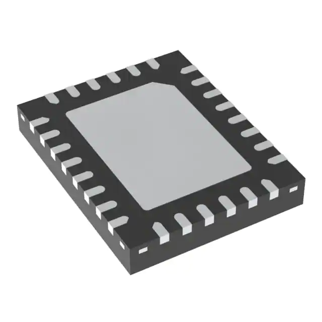
- Part No.:
- ISL97649BIRZ-T
- Manufacturer:
- Renesas
- Category:
- Power Management - Specialized
- Package:
- 28-VFQFN Exposed Pad
- Datasheet:
-
 ISL97649BIRZ-T.pdf
- Description:
- IC POWER MANAGEMENT
- Quantity:
- Payment:

- Shipping:

Inventory:2,513
Please send an inquiry. Send us your inquiry, and we will respond immediately.
Product details
Overview
ISL97649BIRZ-T from Renesas Electronics (formerly Intersil) is an integrated power management IC (PMIC) for TFT-LCD panels in notebooks, tablets, and monitors. It integrates a 1.5A boost converter (600/1200kHz), gate pulse modulator (up to 30V output), VCOM amplifier with 8-bit DCP, supply monitor with reset, and charge-pump-derived VON/VOFF generation - all in a single 28-pin 4×5 QFN package.
For engineers reviewing the ISL97649BIRZ-T datasheet, ISL97649BIRZ-T pinout, ISL97649BIRZ-T application, or ISL97649BIRZ-T equivalent, this page delivers verified technical context, real-world timing and voltage sequencing behavior, confirmed I²C DCP interface details (address 100111), and validated alternative options for LCD bias supply consolidation.
Technical Context
The ISL97649BIRZ-T implements a current-mode PWM boost controller with selectable 600kHz or 1.2MHz switching, using internal 0.18Ω FET and external soft-start capacitor (SS pin) to control ramp-up of peak current limit. Its gate pulse modulator functions as a three-state multiplexer (GND/VGH/GPM_LO) with independent delay (CE pin) and slew-rate (RE pin) control via external RC components.
The integrated VCOM amplifier operates with rail-to-rail input (0–AVDD), ±225mA short-circuit current capability, 25V/µs slew rate, and 20MHz gain bandwidth - optimized for driving large capacitive LCD backplane loads. The DCP uses nonvolatile 8-bit EEPROM storage to retain wiper position across power cycles, with I²C address fixed at 100111 (MSB left).
Key Specifications
| Parameter | Value and Actual Design Meaning |
|---|---|
| VIN Range | 2.5V to 5.5V - supports direct connection to system logic rails (3.3V or 5V) without pre-regulation. |
| AVDD Boost Output | Programmable via FB divider; typical 8.06V - powers internal analog blocks and external charge pumps. |
| Boost Switch FET | 1.5A peak / 0.18Ω RDS(on) - enables high-efficiency conversion with minimal external component count. |
| GPM Output Voltage Range | Up to 30V on VGHM - sufficient for modern TFT gate drivers requiring >25V swing. |
| VCOM Amplifier Output Current | ±225mA short-circuit - handles transient pixel charging demands without latch-up or thermal shutdown under typical display line rates. |
| DCP Resolution & Storage | 8-bit wiper (256 steps), nonvolatile EEPROM - retains last programmed VCOM offset across cold starts. |
| I²C Address | 100111 (7-bit, MSB left) - allows daisy-chaining with other I²C peripherals on same bus without address conflict. |
Pinout & Package
Package: 28-lead 4mm × 5mm QFN with exposed thermal pad (RoHS-compliant, Pb-free). Pin pitch: 0.5mm. Thermal resistance θJA = 38°C/W, θJC = 4.5°C/W.
| Pin/Terminal | Circuit Role | Design Meaning |
|---|---|---|
| FB | AVDD feedback node | Connects to center of resistor divider to set AVDD output voltage; 0.8V reference enables precise regulation. |
| FREQ | Boost frequency select | Pull to GND for 600kHz (lower loss at light load); pull to VIN for 1.2MHz (smaller inductor/capacitor size). |
| VDPM | GPM enable delay control | Capacitor to GND sets delay before gate drive activation; internal 10µA current source charges it to 1.215V threshold. |
| CE | GPM high-to-low delay | Capacitor to GND sets time between VFLK falling edge and VGHM transition start; enables precise blanking timing. |
| RE | GPM slew rate control | Resistor to GND sets falling-edge dv/dt of VGHM; critical for EMI reduction and gate oxide stress mitigation. |
| RSET | DCP sink current calibration | Resistor to GND sets full-scale current for POS pin sink - determines DCP output voltage range and resolution. |
| SCL/SDA | I²C interface | Standard bidirectional bus pins; support 400kHz Fast Mode; internal pull-downs ensure defined state during boot. |
| RESET | Open-drain system reset | Asserted low when VDIV falls below 1.22V; 650Ω internal pull-down ensures clean reset signaling to host controller. |
Key Features
| Feature | Design Value |
|---|---|
| Integrated VCOM calibrator | Combines 8-bit DCP + rail-to-rail VCOM op-amp in one die - eliminates discrete trim pot and external op-amp, reducing BOM and layout area. |
| Programmable gate drive timing | Independent CE (delay) and RE (slew) pins allow fine-tuning of VGHM transitions to match panel-specific timing requirements and reduce EMI. |
| Supply-monitor reset with adjustable delay | CD2 capacitor sets rising-edge delay (e.g., 12.17ms with 100nF); prevents premature MCU wake-up during power ramp. |
| Charge-pump-compatible VON/VOFF generation | LX switching node drives external charge pumps - avoids need for separate high-voltage generators and simplifies VGH/VGL rail design. |
| Robust fault protection | UVLO (2.2–2.4V), OVP (15–16V), OTP (153°C), OCP (1.5A), and UVP - ensures safe operation during abnormal conditions without external supervision. |
Applications
| High-Resolution Notebook Display | Industrial Tablet Panel |
|---|---|
Use Scenario: Driving 1920×1080 IPS LCD with fast response time and wide viewing angle. IC Role / Device Role / Timing Role: Generates AVDD (8V), VON (24V), VOFF (−6V), VCOM (programmable offset), and synchronized gate pulses (VGHM) with controlled slew and delay. Use Value: Single-chip solution reduces PCB area by >40% vs. discrete PMIC + VCOM + gate driver combo; I²C DCP enables factory calibration and field VCOM drift correction. | Use Scenario: Ruggedized 10.1″ tablet used in warehouse scanning with ambient temperature range −20°C to +70°C. IC Role / Device Role / Timing Role: Provides stable VCOM bias and gate drive timing across temperature; supply monitor generates reliable reset during battery brownout events. Use Value: Built-in thermal shutdown (153°C) and extended −40°C to +85°C operating range ensure reliability in uncontrolled environments; nonvolatile DCP preserves calibration after power loss. |
| Medical Monitor LCD | POS Terminal Display |
Use Scenario: 15″ diagnostic-grade monitor requiring flicker-free, color-accurate image rendering. IC Role / Device Role / Timing Role: Delivers ultra-stable VCOM voltage (±2.5mV offset, 75dB CMRR) and precisely timed gate pulses to minimize crosstalk and vertical banding artifacts. Use Value: 25V/µs slew rate and ±225mA drive capability maintain VCOM stability during rapid pixel updates; low-noise AVDD rail minimizes analog supply coupling into VCOM path. | Use Scenario: Compact countertop POS terminal with 7″ resistive touch LCD and limited board space. IC Role / Device Role / Timing Role: Consolidates AVDD boost, VCOM amplification, gate pulse modulation, and reset generation into one 4×5mm footprint. Use Value: Eliminates 5+ discrete ICs and associated passives; QFN thermal pad enables conduction cooling in sealed enclosures without heatsinks. |
Equivalent & Alternatives
The following parts are listed as comparable options for similar TFT-LCD power management applications.
| Alternative Part | Technical Difference | Application Difference | Selection Advice |
|---|---|---|---|
| ISL97649BIRTZ | No tape-and-reel suffix; identical electrical specs and pinout - differs only in packaging format (cut tape vs. reel). | Same functional use in evaluation and low-volume prototyping; not intended for automated SMT assembly. | Select ISL97649BIRTZ for bench validation; ISL97649BIRZ-T is required for production line feeders. |
| RTQ2132B-QT | Single-channel boost + VCOM amp only; lacks integrated gate pulse modulator, VON/VOFF charge-pump drivers, and supply monitor. | Suitable for simpler displays without active gate timing control; requires external gate driver and reset supervisor. | Choose RTQ2132B-QT only if gate pulse modulation and system-level reset are handled elsewhere in design. |
Compared with ISL97649BIRZ-T, ISL97649BIRTZ offers identical functionality in cut-tape form but lacks reel compatibility for high-volume SMT, while RTQ2132B-QT provides partial integration - omitting gate pulse control and system monitoring - making it insufficient as a drop-in replacement for full-feature notebook or tablet LCD bias systems.
Availability
ISL97649BIRZ-T is available at Aetrix Electronics and suitable for high-resolution notebook displays, industrial tablet panels, medical monitor LCDs, and POS terminal displays requiring stable component supply and long-term lifecycle support.
Supply support for ISL97649BIRZ-T includes scheduled delivery planning, volume procurement assistance, BOM continuity management, traceable sourcing, and lifecycle availability coordination for OEM customers, industrial embedded developers, connected-device designers, and electronics production programs.
Manufacturer
Renesas Electronics Corporation is a global semiconductor leader formed from the merger of Renesas Technology and NEC Electronics, specializing in microcontrollers, analog, power, and SoC solutions.
The ISL97649BIRZ-T belongs to Renesas' legacy Intersil LCD PMIC portfolio, designed specifically to consolidate bias supply, gate timing, and VCOM calibration functions for cost-sensitive, space-constrained TFT-LCD applications in portable and industrial displays.
FAQ
What is the I²C address of the ISL97649BIRZ-T DCP interface?
The ISL97649BIRZ-T uses a fixed 7-bit I²C address of 100111 (binary), with MSB transmitted first. This corresponds to 0x4E in hexadecimal when the R/W bit is zero. The address cannot be changed via hardware pins or software configuration, ensuring predictable bus arbitration in multi-peripheral systems. All DCP register reads and writes must target this address to communicate with the ISL97649BIRZ-T's internal digital potentiometer.
How does the ISL97649BIRZ-T handle power-down sequencing for VGHM and VCOM?
During power-down, the ISL97649BIRZ-T forces VGHM to track VGH until VGH drops below 3V, then releases VGHM to float - preventing unintended gate driver behavior. Simultaneously, the VCOM amplifier maintains its last output voltage (set by the 8-bit DCP EEPROM value) until AVDD falls below UVLO, ensuring stable LCD bias during brownout. The RESET pin asserts low when VDIV falls below 1.22V, providing synchronous system reset signaling.
Can the ISL97649BIRZ-T operate with a 5V-only input supply?
Yes, the ISL97649BIRZ-T supports VIN from 2.5V to 5.5V, making it fully compatible with 5V system rails. At VIN = 5V, the boost converter efficiently generates AVDD (e.g., 8.06V) using the internal 1.5A FET and selectable 600kHz/1.2MHz switching. Input decoupling requires only a 0.1µF ceramic capacitor near the VIN pin, and no LDO pre-regulator is needed - simplifying power architecture for 5V-based designs.
What protection features are built into the ISL97649BIRZ-T?
The ISL97649BIRZ-T integrates undervoltage lockout (UVLO: 2.2–2.4V), overvoltage protection (OVP: 15–16V on AVDD), overcurrent protection (OCP: 1.5A peak switch limit), overtemperature shutdown (OTP: 153°C), and undervoltage protection (UVP) on VDIV. These operate autonomously without firmware or external supervision, ensuring fail-safe behavior during fault conditions such as input brownout, output short, or thermal overload - critical for unattended display operation.
Is the ISL97649BIRZ-T still recommended for new designs?
No - the official datasheet states "NOT RECOMMENDED FOR NEW DESIGNS" and lists "NO RECOMMENDED REPLACEMENT". While ISL97649BIRZ-T remains available for legacy support and existing production, Renesas does not endorse it for new projects. Engineers should consult Renesas' Technical Support Center (1-888-INTERSIL or www.intersil.com/tsc) for migration paths to newer LCD PMICs with enhanced efficiency, smaller packages, or updated feature sets before initiating new designs involving ISL97649BIRZ-T.
ISL97649BIRZ-T Specifications
- Product attributes
- Attribute value
- Manufacturer:
- Renesas
- Series:
- -
- Package/Case:
- 28-VFQFN Exposed Pad
- Packaging:
- Tape & Reel (TR)
- Product Status:
- Obsolete
- Applications:
- LCD Display
- Current - Supply:
- 700µA
- Voltage - Supply:
- 2.5V ~ 5.5V
- Operating Temperature:
- -40°C ~ 85°C
- Grade:
- -
- Qualification:
- -
- Mounting Type:
- Surface Mount
- Supplier Device Package:
- 28-QFN (4x5)
ISL97649BIRZ-T FAQ
1.How can I place an order for ISL97649BIRZ-T through Aetrix?
Please submit a Request for Quotation (RFQ) for ISL97649BIRZ-T on Aetrix. Our sales agent will provide a competitive quotation and guide you through the order confirmation once you accept the terms.
2.Are the price and stock information for ISL97649BIRZ-T reliable?
The price and inventory of ISL97649BIRZ-T are updated periodically and may fluctuate due to market conditions. Stock and pricing data are typically refreshed every 24 hours. Quotation validity for ISL97649BIRZ-T is usually 5 days.
3.What payment methods are accepted for ISL97649BIRZ-T?
We accept Wire Transfer, PayPal, Credit Card, Western Union, MoneyGram, and Escrow for ISL97649BIRZ-T transactions.
Note: Certain payment methods may incur a processing fee.
4.How is shipping managed for ISL97649BIRZ-T?
ISL97649BIRZ-T orders can be shipped via leading logistics carriers, including DHL, UPS, FedEx, TNT, or Registered Mail.
Once your ISL97649BIRZ-T order is processed, you will receive an email with the shipment details and tracking number.
Note: Tracking information may take up to 24 hours to appear. Express delivery typically takes 3–5 business days.
5.How can I obtain technical support or documentation for ISL97649BIRZ-T?
For technical support, including ISL97649BIRZ-T datasheets, pinout diagrams, or application guidance, please contact our engineering support team. They can provide detailed documentation and assistance for your ISL97649BIRZ-T requirements.
6.How does Aetrix verify that ISL97649BIRZ-T is sourced from the original manufacturer or authorized distributors?
All ISL97649BIRZ-T products on Aetrix are procured from qualified distributors and authorized channels. Our dedicated quality assurance team conducts strict verification, including traceability checks and, if necessary, third-party testing. This ensures that ISL97649BIRZ-T meets industry standards.
7.What is the process for return or replacement of ISL97649BIRZ-T?
All ISL97649BIRZ-T units undergo pre-shipment inspection (PSI). If there is an issue with ISL97649BIRZ-T, returns or replacements are accepted under the following conditions:
1.Quantity discrepancies, incorrect items, or visible external defects (such as breakage or corrosion), acknowledged by Aetrix.
2.The issue is reported within 90 days of delivery.
3.The ISL97649BIRZ-T part is unused and in its original packaging.
Return procedure for ISL97649BIRZ-T:
1.Submit a request within 90 days.
2.Obtain a Return Material Authorization (RMA) from Aetrix.
ISL97649BIRZ-T Tags

-
TPS2511DGNR
Texas Instruments

-
UTC2000/MG
Microchip Technology

-
TUSB320HAIRWBR
Texas Instruments

-
TPS61252DSGR
Texas Instruments

-
PI5USB30216CXUAEX
Diodes Incorporated

-
SN6501DBVR
Texas Instruments

-
CYPD3177-24LQXQT
Infineon Technologies
-
SN6501QDBVRQ1
Texas Instruments

-
STUSB1600AQTR
STMicroelectronics

-
SN6505BDBVR
Texas Instruments
-
SN6501DBVT
Texas Instruments

-
TPS65150PWPR
Texas Instruments
Tech Hub

TTL and CMOS logic families differ in thresholds, loading, output drive, power and timing. This engineering guide compares 74HC and 74HCT, calculates noise margins and checks 3.3 V/5 V compatibility.

A practical engineering guide to 3.3V and 5V logic compatibility, input thresholds, resistor dividers, translator ICs, MOSFET level shifting, I2C pull-ups, timing limits and power-sequencing risks.

The 74HC595 uses push-pull logic outputs, while the TPIC6B595 uses 50 V open-drain DMOS sinks for higher-power loads. This guide compares timing, current limits, 3.3 V interfacing, load wiring, thermal…

The 74HC595 converts serial data into eight stable parallel outputs. This guide covers pin functions, shift and storage timing, OE and MR behavior, drive-current limits, cascading, voltage compatibilit…

A technical comparison of level-sensitive latches and edge-triggered flip-flops, covering timing windows, setup and hold limits, master–slave operation, time borrowing, race-through, HDL inference and…

A D latch stores one bit while Enable controls when data can pass. This reference covers gate-level operation, truth tables, transparency, setup and hold timing, LE versus OE, common ICs and practical …

An SR latch stores one bit through cross-coupled feedback. This engineering reference covers NOR and NAND implementations, truth tables, forbidden-state recovery, gated operation, switch debouncing, fa…

Latch circuits retain one bit through feedback. This technical reference covers SR and D latches, truth tables, transparency, timing limits, latch-versus-flip-flop behavior, applications and common log…

An engineering guide to LED driver operation, constant-current and constant-voltage outputs, linear and switching topologies, dimming, IC selection, calculations, replacement compatibility, and fault c…

Operational amplifier guide covering op amp basics, feedback, ideal vs real op amps, common configurations, buffer circuits, offset, bias current, gain-bandwidth, slew rate, rail-to-rail limits and sel…


