
 My Inquiry
 My Account


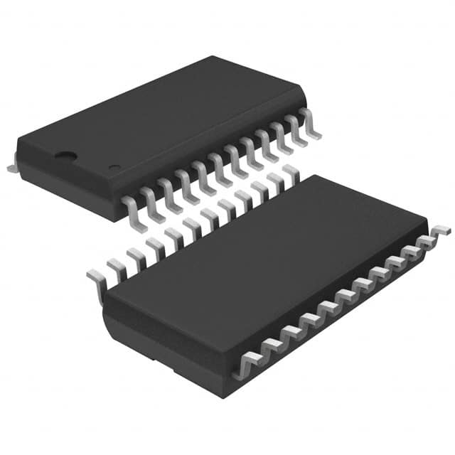
STMicroelectronics L9524C-TR
- Part No.:
- L9524C-TR
- Manufacturer:
- STMicroelectronics
- Category:
- Power Management - Specialized
- Package:
- 24-SOIC (0.295", 7.50mm Width)
- Datasheet:
-
 L9524C-TR.pdf
- Description:
- IC CTRL GLOW PLUG SYSTEM 24-SOIC
- Quantity:
- Payment:

- Shipping:

Inventory:4,795
Please send an inquiry. Send us your inquiry, and we will respond immediately.
Product details
Overview
L9524C-TR from STMicroelectronics is a quad high-side gate driver IC for diesel engine glow plug control, supporting up to six glow plugs via four external N-channel MOSFETs or one relay. It features PWM-controlled gate drive with adjustable charge/discharge current (270–540 µA), overcurrent shutdown (adjustable 150–290 mV threshold), and integrated battery (VBAT), supply (VVS), junction temperature (TJ = 125–150 °C shutdown), and charge pump voltage monitoring. Used in automotive diesel cold-start systems.
For engineers reviewing the L9524C-TR datasheet, L9524C-TR pinout, L9524C-TR application, or L9524C-TR equivalent, this page delivers verified functional context, SO24 package mapping, real-time diagnostic interface behavior, and validated alternatives for diesel engine management system integration.
Technical Context
The L9524C-TR implements a two-wire serial diagnostic interface (DO/CI) compatible with battery voltage (6–18 V), supports six operating modes (relay or transistor sense/shunt sense with/without power regulation), and uses internal charge pump (0.6–7 MHz) to drive high-side MOSFET gates above VS rail. It distinguishes shunt-based vs. RDS(on)-based current sensing with temperature-compensated overcurrent thresholds.
Its gate drivers (G1–G4) provide clamped output (−18 V min), negative inductive load clamping, and advanced run-off control timing (tgap = 50–250 µs). Power regulation in Modes 4/6 dynamically adjusts PWM duty cycle based on real-time VBAT feedback to maintain constant glow plug power across battery variations (8–16 V).
Key Specifications
| Parameter | Value and Actual Design Meaning |
|---|---|
| Supply voltage (VS) | −0.3 to 45 V; undervoltage lockout at 4–5 V with 100–400 mV hysteresis ensures safe startup. |
| Battery monitoring (BAT) | Detects battery undervoltage (1–2 V threshold) in Modes 2–6 to flag fuse/open-circuit faults. |
| Gate drive current | Adjustable 270–540 µA charge/discharge (via CUR pin); enables optimized MOSFET switching speed and EMI control. |
| Overcurrent threshold | Configurable 150–290 mV (shunt/transistor sense); triggers shutdown within 400–950 µs filter window. |
| Junction temp shutdown | Activates at 125–150 °C; prevents thermal runaway during sustained high-power glow plug operation. |
| Diagnostic interface | Two-wire serial protocol (CI/DO); supports go/no-go and full serial diagnostics per AEC-Q100 automotive requirements. |
| Charge pump output (CP) | Generates VVS + 5 to VVS + 18 V; powers high-side gate drivers independently of VS rail limitations. |
Pinout & Package
Package: SO24 (Small Outline, 24-pin, 0.75 mm pitch, body size 15.4 × 7.5 mm, JEDEC MS-013AC). RoHS-compliant, AEC-Q100 qualified for automotive under-hood use.
| Pin/Terminal | Circuit Role | Design Meaning |
|---|---|---|
| 1 SP1 | Positive sense input (glow plug 1) | High-side current sense node for shunt-based monitoring; referenced to SN1. |
| 2 G1 | Gate driver output (channel 1) | Drives external N-MOSFET source; clamped −18 V for inductive kickback protection. |
| 3 SN1 | Negative sense input (glow plug 1) | Low-side return path for SP1; enables differential current measurement. |
| 4 SP2 | Positive sense input (glow plugs 2 & 5) | Shared sense node reduces component count; requires matched layout for accuracy. |
| 5 G2 | Gate driver output (channel 2) | Independent PWM-controlled output; synchronized with G1–G4 via internal timing logic. |
| 6 SN5 | Negative sense input (glow plug 5) | Enables dual-glow-plug monitoring on shared SP2; supports fault isolation. |
| 7 SN2 | Negative sense input (glow plug 2) | Paired with SP2; allows independent open-load detection per channel. |
| 8 BAT | Battery voltage input | Provides auxiliary supply and VBAT feedback for power regulation and fuse monitoring. |
| 9 DO | Diagnostic output | Open-drain serial data line; transmits failure codes and status per AEC-Q100 diagnostic protocol. |
| 10 VS | Main supply input | Primary power rail (−0.3 to 45 V); monitored for UV/OV/load dump events with programmable delays. |
| 11 CP | Charge pump output | Drives external capacitor to generate boosted gate voltage; critical for high-side N-MOSFET turn-on. |
| 12 OCT | Overcurrent threshold setting | Analog input (0–VCUR); sets 150–290 mV trip point with temperature compensation. |
| 13 IO | Mode-select / relay driver output | In relay mode: drives external relay driver; in transistor mode: configures power regulation enable. |
| 14 CUR | Gate charge/discharge current setting | Sets 270–540 µA drive strength; directly scales MOSFET switching speed and gate loss. |
| 15 MS | Mode selection input | Voltage threshold (1–2 V) selects relay vs. transistor mode; determines CI/DO protocol behavior. |
| 16 GND | Ground reference | Common return for all analog/digital functions; requires low-impedance PCB plane for noise immunity. |
| 17 CI | Control input | PWM input (0.4·VVS/0.6·VVS thresholds); falling edge initiates glow plug activation sequence. |
| 18 SN4 | Negative sense input (glow plug 4) | Paired with SP4; supports 6-glow-plug configuration with shared sense nodes. |
| 19 SN6 | Negative sense input (glow plug 6) | Completes 6-plug monitoring set; enables per-plug open-load and overcurrent diagnostics. |
| 20 G4 | Gate driver output (channel 4) | Final high-side driver; supports staggered timing (tgap = 50–250 µs) to reduce peak current draw. |
| 21 SP4 | Positive sense input (glow plugs 4 & 6) | Shared node for compact layout; requires matched trace lengths to avoid measurement error. |
| 22 SN3 | Negative sense input (glow plug 3) | Paired with SP3; completes independent monitoring for all six glow plugs. |
| 23 G3 | Gate driver output (channel 3) | Third driver channel; supports sequential or parallel activation per engine calibration. |
| 24 SP3 | Positive sense input (glow plug 3) | Dedicated sense node for glow plug 3; enables precise individual fault detection. |
Key Features
| Feature | Design Value |
|---|---|
| Quad high-side gate drivers | Four independent PWM outputs (G1–G4) with programmable slew rate and −18 V clamp for inductive load safety. |
| Adjustable overcurrent protection | OCT pin sets 150–290 mV threshold with temperature compensation-enables robust glow plug current limiting across ambient range. |
| Two-wire battery-compatible interface | CI/DO pins operate from 6–18 V battery rails without level-shifting; simplifies ECU interconnect and reduces BOM cost. |
| Power regulation with VBAT feedback | Modes 4/6 dynamically adjust PWM duty cycle using real-time VBAT to maintain constant glow plug power despite battery sag. |
| Advanced run-off control | Staggered channel deactivation (tgap = 50–250 µs) minimizes inrush current and avoids simultaneous MOSFET turn-off stress. |
| Integrated multi-fault monitoring | Simultaneous monitoring of VVS, VBAT, TJ, CP, glow plug currents, and external switches-reduces need for external supervisory ICs. |
Applications
| Diesel Cold-Start System | Glow Plug Diagnostic Module |
|---|---|
|
Use Scenario: Diesel engine cold cranking below −20 °C requiring precise pre-heating of six glow plugs before ignition. IC Role / Device Role / Timing Role: Central controller managing PWM timing, power regulation, and real-time current monitoring across all six glow plugs. Use Value: Maintains consistent glow plug energy delivery (±1.5% VRMS accuracy) despite battery voltage drop from 12.6 V to 8.5 V during cranking. |
Use Scenario: Aftermarket diagnostic tool verifying glow plug circuit integrity and detecting open/short faults in service workshops. IC Role / Device Role / Timing Role: Generates standardized serial diagnostic messages (via DO) reporting individual channel failures and thermal events. Use Value: Enables fast isolation of failed glow plugs (open-load detection <2 ms) and identification of defective external MOSFETs or wiring. |
| Commercial Vehicle Engine Control Unit | Off-Highway Equipment Glow Management |
|
Use Scenario: Heavy-duty truck ECU managing glow plug sequencing across multiple cylinder banks with strict EMI and thermal constraints. IC Role / Device Role / Timing Role: High-side driver with staggered channel timing (50–250 µs gap) to limit peak current and meet CISPR 25 Class 5 emissions. Use Value: Eliminates need for discrete gate drivers and current sense amplifiers-reducing board space by >35% and component count by 12+ parts. |
Use Scenario: Construction equipment operating in extreme ambient temperatures (−40 to +125 °C) requiring reliable glow plug activation in dusty, vibration-prone environments. IC Role / Device Role / Timing Role: Junction temperature monitoring (125–150 °C shutdown) and charge pump voltage supervision ensure fail-safe operation during prolonged idling. Use Value: Prevents thermal damage during extended pre-heat cycles; maintains functionality even with 15% battery voltage ripple (load dump tolerance up to 35 V). |
Equivalent & Alternatives
The following parts are listed as comparable options for similar glow plug control applications.
| Alternative Part | Technical Difference | Application Difference | Selection Advice |
|---|---|---|---|
| INFINEON TLE7209-2R | Single-channel high-side driver; lacks integrated current sense, VBAT monitoring, and multi-mode serial interface. | Requires external current sense amps and microcontroller for diagnostics; suitable only for simple single-glow-plug systems. | Select when cost-sensitive designs need basic high-side drive without integrated diagnostics or multi-plug support. |
| NXP MC33816 | Eight-channel driver with SPI interface; no built-in charge pump-requires external boost for high-side N-MOSFETs. | Supports more channels but demands additional power stage components; diagnostic protocol differs (SPI vs. 2-wire serial). | Select for scalable multi-engine platforms where SPI integration and higher channel count outweigh added BOM complexity. |
Compared with TLE7209-2R and MC33816, the L9524C-TR uniquely integrates charge pump generation, battery-referenced two-wire diagnostics, and six-glow-plug current monitoring in a single SO24 package-reducing system-level validation effort and enabling AEC-Q100-compliant diesel cold-start solutions with minimal external components.
Availability
L9524C-TR is available at Aetrix Electronics and suitable for diesel engine control units, commercial vehicle ECUs, and off-highway equipment requiring stable component supply, AEC-Q100 qualification, and long-term automotive lifecycle support.
Supply support for L9524C-TR includes scheduled delivery planning, volume procurement assistance, BOM continuity management, traceable sourcing, and lifecycle availability coordination for OEM customers, industrial embedded developers, connected-device designers, and electronics production programs.
Manufacturer
STMicroelectronics is a global semiconductor leader specializing in automotive-grade analog, power, and microcontroller solutions with ISO/TS 16949-certified manufacturing.
The L9524C-TR belongs to ST's Automotive Power Switches & Drivers product line, designed specifically for intelligent high-side control in diesel and gasoline engine management systems with integrated diagnostics and functional safety support.
FAQ
What is the maximum number of glow plugs supported by the L9524C-TR?
The L9524C-TR controls up to six glow plugs using four high-side gate drivers (G1–G4) and flexible sense pin mapping: SP1/SN1 (plug 1), SP2/SN2+SN5 (plugs 2 & 5), SP3/SN3 (plug 3), and SP4/SN4+SN6 (plugs 4 & 6). This configuration enables full per-plug monitoring without additional external circuitry.
How does the L9524C-TR handle load dump conditions?
Under load dump (VVS ≥ 28–35 V), the L9524C-TR activates active clamping within 10 µs, turning on all glow plugs to dissipate excess energy. Glow plugs remain energized until VVS drops below the overvoltage threshold (18–22 V) for ≥2 ms-preventing latch-up and ensuring system survival per ISO 7637-2 Pulse 5a.
Can the L9524C-TR operate without an external charge pump capacitor?
No. The CP pin requires an external storage capacitor (typically 1–10 µF, rated ≥35 V) to generate the boosted voltage (VVS + 5 to VVS + 18 V) needed to fully enhance external N-channel MOSFETs in high-side configuration. Omitting this capacitor disables gate drive capability and triggers immediate charge pump undervoltage shutdown.
What diagnostic protocols does the L9524C-TR support on the DO pin?
The DO pin supports two protocols: go/no-go (Mode 1, relay-only) for simple pass/fail reporting, and serial protocol (Modes 2–6) delivering detailed 8-bit failure codes-including open-load, overcurrent, thermal, supply, and switch defect flags-via Manchester-encoded bitstream synchronized to CI edges.
L9524C-TR Specifications
- Product attributes
- Attribute value
- Manufacturer:
- STMicroelectronics
- Series:
- -
- Package/Case:
- 24-SOIC (0.295", 7.50mm Width)
- Packaging:
- Tape & Reel (TR)
- Product Status:
- Active
- Applications:
- Glow Plug Control
- Current - Supply:
- 5mA
- Voltage - Supply:
- 5V ~ 18V
- Operating Temperature:
- -40°C ~ 125°C
- Grade:
- -
- Qualification:
- -
- Mounting Type:
- Surface Mount
- Supplier Device Package:
- 24-SO
L9524C-TR FAQ
1.How can I place an order for L9524C-TR through Aetrix?
Please submit a Request for Quotation (RFQ) for L9524C-TR on Aetrix. Our sales agent will provide a competitive quotation and guide you through the order confirmation once you accept the terms.
2.Are the price and stock information for L9524C-TR reliable?
The price and inventory of L9524C-TR are updated periodically and may fluctuate due to market conditions. Stock and pricing data are typically refreshed every 24 hours. Quotation validity for L9524C-TR is usually 5 days.
3.What payment methods are accepted for L9524C-TR?
We accept Wire Transfer, PayPal, Credit Card, Western Union, MoneyGram, and Escrow for L9524C-TR transactions.
Note: Certain payment methods may incur a processing fee.
4.How is shipping managed for L9524C-TR?
L9524C-TR orders can be shipped via leading logistics carriers, including DHL, UPS, FedEx, TNT, or Registered Mail.
Once your L9524C-TR order is processed, you will receive an email with the shipment details and tracking number.
Note: Tracking information may take up to 24 hours to appear. Express delivery typically takes 3–5 business days.
5.How can I obtain technical support or documentation for L9524C-TR?
For technical support, including L9524C-TR datasheets, pinout diagrams, or application guidance, please contact our engineering support team. They can provide detailed documentation and assistance for your L9524C-TR requirements.
6.How does Aetrix verify that L9524C-TR is sourced from the original manufacturer or authorized distributors?
All L9524C-TR products on Aetrix are procured from qualified distributors and authorized channels. Our dedicated quality assurance team conducts strict verification, including traceability checks and, if necessary, third-party testing. This ensures that L9524C-TR meets industry standards.
7.What is the process for return or replacement of L9524C-TR?
All L9524C-TR units undergo pre-shipment inspection (PSI). If there is an issue with L9524C-TR, returns or replacements are accepted under the following conditions:
1.Quantity discrepancies, incorrect items, or visible external defects (such as breakage or corrosion), acknowledged by Aetrix.
2.The issue is reported within 90 days of delivery.
3.The L9524C-TR part is unused and in its original packaging.
Return procedure for L9524C-TR:
1.Submit a request within 90 days.
2.Obtain a Return Material Authorization (RMA) from Aetrix.
L9524C-TR Tags

-
TPS2511DGNR
Texas Instruments

-
UTC2000/MG
Microchip Technology

-
TUSB320HAIRWBR
Texas Instruments

-
TPS61252DSGR
Texas Instruments

-
PI5USB30216CXUAEX
Diodes Incorporated

-
SN6501DBVR
Texas Instruments

-
CYPD3177-24LQXQT
Infineon Technologies
-
SN6501QDBVRQ1
Texas Instruments

-
STUSB1600AQTR
STMicroelectronics

-
SN6505BDBVR
Texas Instruments
-
SN6501DBVT
Texas Instruments

-
TPS65150PWPR
Texas Instruments
Tech Hub

A practical engineering and sourcing framework covering lifecycle verification, lifetime-buy calculations, replacement qualification, supplier checks and counterfeit-risk controls.

TTL and CMOS logic families differ in thresholds, loading, output drive, power and timing. This engineering guide compares 74HC and 74HCT, calculates noise margins and checks 3.3 V/5 V compatibility.

A practical engineering guide to 3.3V and 5V logic compatibility, input thresholds, resistor dividers, translator ICs, MOSFET level shifting, I2C pull-ups, timing limits and power-sequencing risks.

The 74HC595 uses push-pull logic outputs, while the TPIC6B595 uses 50 V open-drain DMOS sinks for higher-power loads. This guide compares timing, current limits, 3.3 V interfacing, load wiring, thermal…

The 74HC595 converts serial data into eight stable parallel outputs. This guide covers pin functions, shift and storage timing, OE and MR behavior, drive-current limits, cascading, voltage compatibilit…

A technical comparison of level-sensitive latches and edge-triggered flip-flops, covering timing windows, setup and hold limits, master–slave operation, time borrowing, race-through, HDL inference and…

A D latch stores one bit while Enable controls when data can pass. This reference covers gate-level operation, truth tables, transparency, setup and hold timing, LE versus OE, common ICs and practical …

An SR latch stores one bit through cross-coupled feedback. This engineering reference covers NOR and NAND implementations, truth tables, forbidden-state recovery, gated operation, switch debouncing, fa…

Latch circuits retain one bit through feedback. This technical reference covers SR and D latches, truth tables, transparency, timing limits, latch-versus-flip-flop behavior, applications and common log…

An engineering guide to LED driver operation, constant-current and constant-voltage outputs, linear and switching topologies, dimming, IC selection, calculations, replacement compatibility, and fault c…


