
 My Inquiry
 My Account


STMicroelectronics L9779WD-SPI
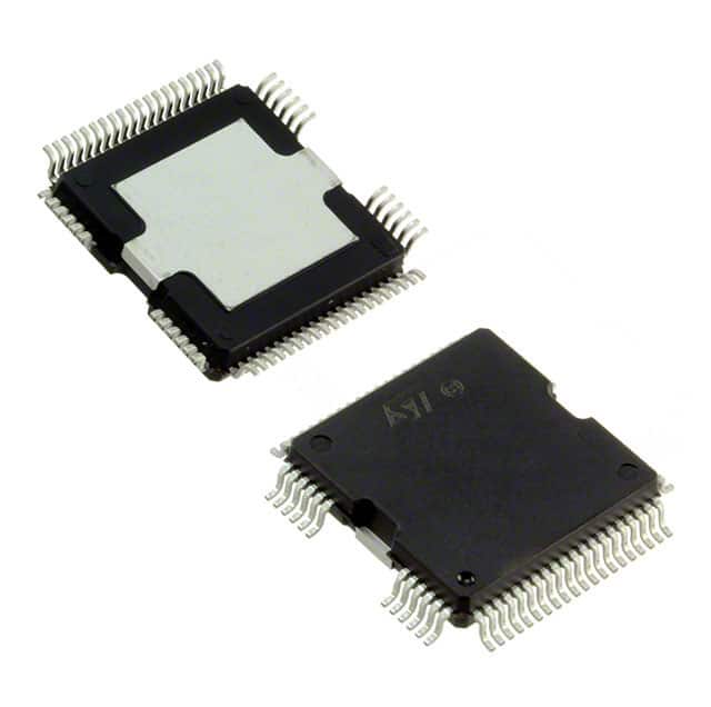
- Part No.:
- L9779WD-SPI
- Manufacturer:
- STMicroelectronics
- Category:
- Power Management - Specialized
- Package:
- 64-BQFP Exposed Pad
- Datasheet:
-
 L9779WD-SPI.pdf
- Description:
- MULTIFUNCTION IC FOR ENGINE MANA
- Quantity:
- Payment:

- Shipping:

Inventory:474
Please send an inquiry. Send us your inquiry, and we will respond immediately.
Product details
Overview
L9779WD-SPI from STMicroelectronics is a multifunction automotive IC for engine management systems, integrating 5 V and 3.3 V logic regulators, 5 V tracking sensor supply, high-speed CAN transceiver, ISO9141 K-Line interface, and protected low-side drivers (OUT1–OUT20) plus IGBT pre-drivers (IGN1–IGN4). It implements Secure Engine Off (SEO), adaptive flying wheel (VRS) sensing, thermal shutdown, and VDA 2.0-compliant 3-level watchdog in BCD6S technology.
For engineers reviewing the L9779WD-SPI datasheet, L9779WD-SPI pinout, L9779WD-SPI application in engine control units, or L9779WD-SPI equivalent for power stage consolidation, this device delivers integrated power management, diagnostics, and communication interfaces tailored to ISO 26262 ASIL-B–capable engine ECU architectures.
Technical Context
The L9779WD-SPI integrates six functional domains: dual linear regulators (5 V/300 mA, 3.3 V/200 mA), configurable power stages (CPS) supporting stepper motor drive or H-bridge/low-side configurations, adaptive VRS front-end with auto-tuning amplitude/time thresholds, and dual serial interfaces (SPI + ISO9141 + high-speed CAN). All subsystems are coordinated by a centralized monitoring module featuring VDA 2.0–compliant triple-watchdog architecture.
Its power-up/down management unit enforces deterministic sequencing across VB (battery), VDD5, and VDD33 rails, while the Smart Reset circuit enables controlled driver switch-off via Power Latch with SEO functionality. Diagnostics cover open-load, short-to-battery, short-to-ground, and overtemperature detection per output channel, reported via SPI registers DIA_REG1–DIA_REG15.
Key Specifications
| Parameter | Value and Actual Design Meaning |
|---|---|
| Logic Regulators | 5 V / 300 mA and 3.3 V / 200 mA linear regulators - supply MCU, sensors, and logic peripherals with tight load regulation (±2%) and built-in thermal foldback. |
| Sensor Supply | 5 V tracking supply (±1% accuracy, 100 mA max) - maintains precise bias for crank/cam position sensors under battery variation (5.5–27 V). |
| CAN Interface | High-speed CAN transceiver (ISO 11898-2 compliant, 1 Mbps max) - supports direct connection to vehicle CAN bus without external level-shifting or termination. |
| VRS Input | Flying wheel interface with adaptive time/amplitude control - automatically adjusts filtering thresholds to detect variable-reluctance signals across RPM ranges (0–20,000 rpm) and air gaps (0.3–2 mm). |
| Output Drivers | 20 protected low-side outputs: OUT1–4 (injectors, 1.5 A peak), OUT5–7 (O₂ heaters, 3 A), OUT13–18 (relays, 2.5 A), OUT20 (low-current, 100 mA); all with current limiting, diagnostics, and thermal shutdown. |
| Watchdog | VDA 2.0–compliant 3-level watchdog (WDA, AB1, WD_RST) - provides independent fault detection paths with configurable timeouts and reset propagation for ASIL-B system integrity. |
| Package | HiQUAD-64 (10 × 10 mm, 1.45 mm height, exposed thermal pad) - optimized for automotive under-hood thermal dissipation (RθJA = 28 °C/W, RθJC = 2.5 °C/W). |
Pinout & Package
Supplied in HiQUAD-64 package: thermally enhanced QFN with 64 leads, exposed die paddle, and wettable flanks for automated optical inspection. Pin layout follows standardized automotive power IC topology with grouped power, ground, analog input, and digital I/O sections.
| Pin/Terminal | Circuit Role | Design Meaning |
|---|---|---|
| VDD5 | 5 V regulator output | Primary logic rail for internal digital blocks and external MCU core; monitored for undervoltage lockout and brownout detection. |
| VDD33 | 3.3 V regulator output | Secondary logic rail for peripherals and ADC reference; isolated from VDD5 to prevent coupling noise into sensitive analog circuits. |
| VB | Battery input (5.5–27 V) | Main power source feeding all regulators and drivers; includes load-dump protection (40 V/100 ms) and reverse-battery tolerance (−24 V/1 s). |
| VRS_IN | Flying wheel sensor input | Differential analog input with programmable gain and adaptive thresholding - accepts ±50 mV to ±1 V peak-to-peak VR signals without external conditioning. |
| IGN1–IGN4 | IGBT pre-driver outputs | Open-drain N-channel outputs driving external IGBT gates; support parallel input configuration for synchronized ignition timing. |
| OUT1–OUT20 | Protected low-side driver outputs | Individually controllable, current-limited, and diagnosable switches - each reports fault status via dedicated SPI diagnostic registers. |
| SPI_MOSI/MISO/SCK/CS | SPI interface signals | 16-bit frame, 4-wire master/slave interface operating up to 10 MHz - used for configuration, real-time status readback, and firmware updates. |
| CAN_H/CAN_L | CAN bus differential pair | Direct connection to vehicle CAN network; integrated common-mode choke and dominant/recessive voltage clamping meet ISO 11898-2 EMC requirements. |
Key Features
| Feature | Design Value |
|---|---|
| Secure Engine Off (SEO) | Power latch ensures safe, sequenced deactivation of all outputs during key-off - prevents uncontrolled fuel cut or spark interruption that could damage catalytic converters. |
| Adaptive VRS Sensing | Auto-calibrates amplitude and timing thresholds per engine cycle - eliminates manual tuning for varying sensor air gaps, wear, or temperature drift across lifetime. |
| Configurable Power Stages (CPS) | Four CPS channels (OUTA–OUTD) reconfigurable as H-bridges, half-bridges, or single low-side drivers - supports stepper motor control, fan actuation, or valve positioning without external components. |
| VDA 2.0 Watchdog | Three independent watchdog timers (WDA algorithmic, AB1 hardware, WD_RST reset path) - enables layered safety monitoring aligned with ISO 26262 ASIL-B decomposition requirements. |
| Integrated Diagnostics | Per-output open-load, short-to-battery, short-to-ground, and overtemperature reporting via 15 dedicated SPI diagnostic registers - reduces need for external sense resistors or comparators. |
Applications
| Engine Control Unit (ECU) | Transmission Control Module (TCM) |
|---|---|
|
Use Scenario: Centralized power management and actuator control in gasoline/diesel engine ECUs. IC Role / Device Role / Timing Role: Multifunction system basis chip providing regulated supplies, injector/ignition drive, VRS signal conditioning, and CAN/K-Line communication. Use Value: Reduces BOM count by consolidating 12+ discrete regulators, drivers, and interface ICs into one HiQUAD-64 package with unified diagnostics and safety monitoring. |
Use Scenario: Valve timing and solenoid control in 8-speed automatic transmissions. IC Role / Device Role / Timing Role: Configurable power stage (CPS) driver for cam phaser actuators and shift solenoids, with real-time current feedback and thermal derating. Use Value: Enables precise PWM-controlled torque delivery to hydraulic valves using OUTA–OUTD in half-bridge mode, with built-in overcurrent shutdown preventing coil burnout. |
| Exhaust Aftertreatment System | On-Board Diagnostics (OBD-II) |
|
Use Scenario: O₂ heater control and NOₓ sensor biasing in diesel exhaust fluid (DEF) dosing systems. IC Role / Device Role / Timing Role: Protected low-side driver (OUT5–OUT7) delivering 3 A pulsed current to O₂ heater elements, with closed-loop temperature compensation. Use Value: Maintains optimal sensor operating temperature (700–800 °C) within 2 seconds of cold start, meeting Euro 6d OBD-II readiness monitor timing requirements. |
Use Scenario: Standardized diagnostic communication between ECU and scan tool via vehicle data link connector (DLC). IC Role / Device Role / Timing Role: Dual-protocol serial interface (ISO9141 K-Line + high-speed CAN) enabling legacy and modern OBD-II session handling. Use Value: Eliminates need for external protocol translator ICs - supports both slow-init (K-Line) and fast-init (CAN) diagnostic modes on same hardware platform. |
Equivalent & Alternatives
The following parts are listed as comparable options for similar multifunction automotive power management applications.
| Alternative Part | Technical Difference | Application Difference | Selection Advice |
|---|---|---|---|
| NXP MC33816 | Single 5 V regulator (400 mA), no 3.3 V rail; lacks VRS interface and CPS configurability; uses SPI + LIN instead of K-Line + CAN. | Targeted at mid-tier ECUs with simpler sensor sets and LIN-based diagnostics; not suitable for VRS-crank sensing or stepper motor control. | Select when cost-sensitive designs omit O₂ heater drivers and require only LIN diagnostics - avoids over-specification of unused features. |
| Renesas RH850/P1M | MCU with integrated power management IP (not standalone IC); requires external gate drivers for IGBTs; no dedicated VRS front-end or SEO latch. | Used in highly integrated ECU SoCs where software-defined timing and diagnostics replace fixed-function hardware blocks. | Choose for scalable software-defined engine control platforms - trades hardware diagnostic depth for firmware flexibility and multi-core processing. |
Compared with MC33816 and RH850/P1M, the L9779WD-SPI uniquely combines dual regulated rails, adaptive VRS sensing, SEO latch, and full CAN/K-Line connectivity in a single package - making it optimal for ASIL-B engine ECUs requiring hardware-enforced safety and minimal external component count.
Availability
L9779WD-SPI is available at Aetrix Electronics and suitable for engine control units, transmission control modules, exhaust aftertreatment systems, and OBD-II diagnostic interfaces requiring stable component supply across automotive production lifecycles (15+ years).
Supply support for L9779WD-SPI includes scheduled delivery planning, volume procurement assistance, BOM continuity management, traceable sourcing, and lifecycle availability coordination for OEM customers, industrial embedded developers, connected-device designers, and electronics production programs.
Manufacturer
STMicroelectronics is a global semiconductor leader headquartered in Geneva, Switzerland, specializing in automotive, industrial, and power management ICs with vertical manufacturing capability and AEC-Q100 qualification expertise.
The L9779WD-SPI belongs to ST's SPC5 family of system basis chips (SBCs), designed specifically for ASIL-B–compliant engine and powertrain ECUs needing consolidated power, communication, and actuator drive functions in harsh automotive environments.
FAQ
What is the maximum allowable supply voltage for the VB pin?
The VB pin supports operation from 5.5 V to 27 V under normal conditions, with transient tolerance up to 40 V for 100 ms (load dump) and −24 V for 1 s (reverse battery). These ratings are validated per ISO 7637-2 Pulse 5a and ISO 16750-2, ensuring robustness in 12 V and 24 V vehicle electrical systems without external protection circuitry.
How does the adaptive VRS interface handle variable air gaps?
The VRS interface continuously monitors signal amplitude and zero-crossing timing during engine rotation, dynamically adjusting internal comparator thresholds and filter time constants. This auto-adaptation compensates for air gap variations from 0.3 mm to 2 mm and maintains reliable crankshaft position detection across temperature (−40 °C to 150 °C) and aging effects without recalibration.
Can the CPS channels be used for bidirectional motor control?
Yes - when configured as H-bridges (via CONFIG_REG10), OUTA–OUTD support full bidirectional control of DC or stepper motors. Each bridge provides independent PWM input, current sense feedback, and cross-conduction prevention logic, enabling precise speed and position control without external gate drivers or external current sensing.
Is the L9779WD-SPI qualified for automotive safety standards?
Yes - the device meets AEC-Q100 Grade 1 (−40 °C to +125 °C ambient) and supports ISO 26262 ASIL-B system integration through its VDA 2.0–compliant triple-watchdog architecture, diagnostic coverage of all power stages, and hardware-enforced SEO sequence. Safety documentation (FMEDA, FMEA) is available under NDA from STMicroelectronics.
L9779WD-SPI Specifications
- Product attributes
- Attribute value
- Manufacturer:
- STMicroelectronics
- Series:
- -
- Package/Case:
- 64-BQFP Exposed Pad
- Packaging:
- Tray
- Product Status:
- Active
- Applications:
- Engine Management
- Current - Supply:
- 550µA
- Voltage - Supply:
- 4.9V ~ 5.1V
- Operating Temperature:
- -40°C ~ 125°C
- Grade:
- -
- Qualification:
- -
- Mounting Type:
- Surface Mount
- Supplier Device Package:
- 64-HiQUAD
L9779WD-SPI FAQ
1.How can I place an order for L9779WD-SPI through Aetrix?
Please submit a Request for Quotation (RFQ) for L9779WD-SPI on Aetrix. Our sales agent will provide a competitive quotation and guide you through the order confirmation once you accept the terms.
2.Are the price and stock information for L9779WD-SPI reliable?
The price and inventory of L9779WD-SPI are updated periodically and may fluctuate due to market conditions. Stock and pricing data are typically refreshed every 24 hours. Quotation validity for L9779WD-SPI is usually 5 days.
3.What payment methods are accepted for L9779WD-SPI?
We accept Wire Transfer, PayPal, Credit Card, Western Union, MoneyGram, and Escrow for L9779WD-SPI transactions.
Note: Certain payment methods may incur a processing fee.
4.How is shipping managed for L9779WD-SPI?
L9779WD-SPI orders can be shipped via leading logistics carriers, including DHL, UPS, FedEx, TNT, or Registered Mail.
Once your L9779WD-SPI order is processed, you will receive an email with the shipment details and tracking number.
Note: Tracking information may take up to 24 hours to appear. Express delivery typically takes 3–5 business days.
5.How can I obtain technical support or documentation for L9779WD-SPI?
For technical support, including L9779WD-SPI datasheets, pinout diagrams, or application guidance, please contact our engineering support team. They can provide detailed documentation and assistance for your L9779WD-SPI requirements.
6.How does Aetrix verify that L9779WD-SPI is sourced from the original manufacturer or authorized distributors?
All L9779WD-SPI products on Aetrix are procured from qualified distributors and authorized channels. Our dedicated quality assurance team conducts strict verification, including traceability checks and, if necessary, third-party testing. This ensures that L9779WD-SPI meets industry standards.
7.What is the process for return or replacement of L9779WD-SPI?
All L9779WD-SPI units undergo pre-shipment inspection (PSI). If there is an issue with L9779WD-SPI, returns or replacements are accepted under the following conditions:
1.Quantity discrepancies, incorrect items, or visible external defects (such as breakage or corrosion), acknowledged by Aetrix.
2.The issue is reported within 90 days of delivery.
3.The L9779WD-SPI part is unused and in its original packaging.
Return procedure for L9779WD-SPI:
1.Submit a request within 90 days.
2.Obtain a Return Material Authorization (RMA) from Aetrix.
L9779WD-SPI Tags

-
TPS2511DGNR
Texas Instruments

-
UTC2000/MG
Microchip Technology

-
TUSB320HAIRWBR
Texas Instruments

-
TPS61252DSGR
Texas Instruments

-
PI5USB30216CXUAEX
Diodes Incorporated

-
SN6501DBVR
Texas Instruments

-
CYPD3177-24LQXQT
Infineon Technologies
-
SN6501QDBVRQ1
Texas Instruments

-
STUSB1600AQTR
STMicroelectronics

-
SN6505BDBVR
Texas Instruments
-
SN6501DBVT
Texas Instruments

-
TPS65150PWPR
Texas Instruments
Tech Hub

A practical engineering and sourcing framework covering lifecycle verification, lifetime-buy calculations, replacement qualification, supplier checks and counterfeit-risk controls.

TTL and CMOS logic families differ in thresholds, loading, output drive, power and timing. This engineering guide compares 74HC and 74HCT, calculates noise margins and checks 3.3 V/5 V compatibility.

A practical engineering guide to 3.3V and 5V logic compatibility, input thresholds, resistor dividers, translator ICs, MOSFET level shifting, I2C pull-ups, timing limits and power-sequencing risks.

The 74HC595 uses push-pull logic outputs, while the TPIC6B595 uses 50 V open-drain DMOS sinks for higher-power loads. This guide compares timing, current limits, 3.3 V interfacing, load wiring, thermal…

The 74HC595 converts serial data into eight stable parallel outputs. This guide covers pin functions, shift and storage timing, OE and MR behavior, drive-current limits, cascading, voltage compatibilit…

A technical comparison of level-sensitive latches and edge-triggered flip-flops, covering timing windows, setup and hold limits, master–slave operation, time borrowing, race-through, HDL inference and…

A D latch stores one bit while Enable controls when data can pass. This reference covers gate-level operation, truth tables, transparency, setup and hold timing, LE versus OE, common ICs and practical …

An SR latch stores one bit through cross-coupled feedback. This engineering reference covers NOR and NAND implementations, truth tables, forbidden-state recovery, gated operation, switch debouncing, fa…

Latch circuits retain one bit through feedback. This technical reference covers SR and D latches, truth tables, transparency, timing limits, latch-versus-flip-flop behavior, applications and common log…

An engineering guide to LED driver operation, constant-current and constant-voltage outputs, linear and switching topologies, dimming, IC selection, calculations, replacement compatibility, and fault c…


