
 My Inquiry
 My Account


STMicroelectronics L9953LXPTR
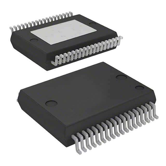
- Part No.:
- L9953LXPTR
- Manufacturer:
- STMicroelectronics
- Category:
- Power Management - Specialized
- Package:
- PowerSSO-36 Exposed Bottom Pad
- Datasheet:
-
 L9953LXPTR.pdf
- Description:
- IC DVR DOOR ACTUATOR POWERSSO36
- Quantity:
- Payment:

- Shipping:

Inventory:2,772
Please send an inquiry. Send us your inquiry, and we will respond immediately.
Product details
Overview
L9953LXPTR from STMicroelectronics is an automotive-grade multifunctional door actuator driver IC integrating five half-bridge outputs (OUT1–OUT5), three high-side drivers (OUT6–OUT8), SPI interface, current monitoring, and programmable soft-start. It delivers 0.75A per half-bridge (RDS(on) = 1600 mΩ), up to 6A on OUT8 (RDS(on) = 100 mΩ), and supports PWM-controlled bidirectional motor driving for door lock, mirror fold/vertical/horizontal control, and defroster/LED lighting. Designed for 12V automotive systems, it operates from −40°C to +150°C junction temperature.
For engineers reviewing the L9953LXPTR datasheet, L9953LXPTR pinout, L9953LXPTR application, or L9953LXPTR equivalent, key selection considerations include its eight-channel configurable output topology (half-bridge vs. high-side), integrated diagnostics (open-load, overload, overtemperature), low standby current (<6 µA), and SPI-configurable soft-start for inrush-current-sensitive loads like incandescent bulbs and DC motors.
Technical Context
The L9953LXPTR implements a microcontroller-driven architecture with a standard 24-bit SPI interface for command input (forward/reverse/brake/hi-Z) and diagnostic status readback. All eight outputs feature independent protection: short-circuit, open-load, overload, and thermal shutdown (Tj = 170°C turn-off, 150°C hysteresis).
It supports dual supply operation (VS = 7–28 V for power stage, VCC = 4.5–5.3 V for logic), includes a charge pump (CP) output for external reverse-polarity MOSFET gate drive, and provides current monitor outputs (CM) for OUT1, OUT4, OUT5, and OUT8 with 1:10,000 scaling and ±4% accuracy at full scale. PWM1 and CM/PWM2 enable external PWM control of multiple outputs.
Key Specifications
| Parameter | Value and Actual Design Meaning |
|---|---|
| Output Configuration | 5 half-bridges (OUT1–OUT5) + 3 high-side drivers (OUT6–OUT8); enables simultaneous control of 3 DC motors + 3 resistive loads |
| Max Output Current | ±10.5 A (OUT4/OUT5 sink/source), ±6 A (OUT8 sink), ±1.25 A (OUT1–OUT3 sink/source); defines motor torque and bulb/LED drive capability |
| RDS(on) (Typ) | 100 mΩ (OUT8), 150 mΩ (OUT4/OUT5), 500 mΩ (OUT6/OUT7 low-R mode), 1600 mΩ (OUT1–OUT3); determines conduction loss and thermal design margin |
| Standby Current | <6 µA (Tj ≤ 85°C); enables ultra-low-power sleep mode for battery-sensitive automotive body modules |
| Diagnostic Coverage | Open-load, overload, overtemperature (130°C warning, 170°C shutdown), short-circuit, and cross-current protection on all outputs |
| SPI Interface | 24-bit serial command/status register; enables real-time configuration and fault reporting without additional GPIO overhead |
| Operating Temp | −40°C to +150°C junction temperature; qualified for under-hood and door module environments |
Pinout & Package
Package: PowerSSO-36 (exposed thermal pad, RoHS-compliant, ECOPACK®). Dimensions: 10.0 mm × 7.5 mm × 1.75 mm (max height), thermal resistance RθJA = 30°C/W (JEDEC Std 51-7, 4-layer board).
| Pin | Circuit Role | Design Meaning |
|---|---|---|
| 1, 18, 19, 36 | GND | Power ground reference; all four pins must be externally connected to handle full output current and minimize ground bounce |
| 2, 35 | OUT8 | High-side driver output (6 A max, RDS(on) = 100 mΩ); intended for mirror defroster or 10W bulb/LED load |
| 3–5, 16–17, 23–24, 30–31 | OUT1–OUT5 | Half-bridge outputs (0.75 A / 6 A capable); OUT1–OUT3 for door lock/mirror axis; OUT4–OUT5 for mirror fold/auxiliary loads |
| 26 | CP | Charge pump output (VS+6 to VS+13 V); drives gate of external N-MOS for reverse polarity protection |
| 8, 11, 13 | DI, DO, CLK | SPI data in/out and clock; CMOS-level, 24-bit frame sync; DO is 3-state when CSN high |
| 10 | CSN | Active-low chip select; >7.5 V triggers test mode; enables SPI communication and disables outputs when high |
| 27 | PWM1 | External PWM input controlling OUT1–OUT6 and OUT8; allows analog dimming or speed modulation without SPI overhead |
| 9 | CM/PWM2 | Bidirectional pin: current monitor output (1:10,000 scaling) for OUT1/OUT4/OUT5/OUT8 OR second PWM input for OUT7 |
Key Features
| Feature | Design Value |
|---|---|
| Programmable Soft Start | Configurable delay and ramp rate for OUT1–OUT8; prevents inrush current damage to incandescent bulbs and motor windings during cold start |
| Integrated Current Monitoring | Real-time analog current sense on four outputs (OUT1, OUT4, OUT5, OUT8) with ±4% accuracy; eliminates need for external shunt amplifiers |
| Dual Supply Architecture | Independent VS (7–28 V) and VCC (4.5–5.3 V) rails; isolates high-noise power stage from sensitive logic, improving EMI resilience |
| Comprehensive Diagnostics | Per-output open-load detection (via pull-up/pull-down test), overload flagging, and thermal warning (130°C) + shutdown (170°C) |
| Reverse Polarity Protection Support | On-chip charge pump (CP) output drives external N-MOS gate; enables robust, low-loss reverse-battery protection without discrete diode drop |
Applications
| Door Lock Actuation | Mirror Fold Control |
|---|---|
|
Use Scenario: Electromechanical locking/unlocking of vehicle doors via solenoid or small DC motor. IC Role / Device Role / Timing Role: Half-bridge driver (OUT1–OUT3) provides bidirectional current to lock/unlock motor; SPI configures direction and braking. Use Value: Integrated open-load diagnosis confirms mechanical jam or broken linkage; soft-start prevents solenoid coil stress during repeated actuation. |
Use Scenario: Motorized folding/unfolding of side mirrors for parking or storage. IC Role / Device Role / Timing Role: Half-bridge (OUT4–OUT5) drives reversible mirror fold motor; PWM1 enables variable-speed control. Use Value: Overload detection halts motion if mirror hits obstacle; current monitor feedback enables position estimation via motor current profile. |
| Mirror Defroster Drive | 10W LED/Bulb Lighting |
|
Use Scenario: Resistive heating element activation on mirror glass to clear condensation/frost. IC Role / Device Role / Timing Role: High-side driver (OUT8) switches 6 A to defroster trace; charge pump (CP) enables reverse-polarity protection. Use Value: Low RDS(on) (100 mΩ) minimizes self-heating during sustained 10W operation; overtemperature shutdown prevents thermal runaway. |
Use Scenario: Interior or exterior lighting using 10W incandescent bulbs or high-brightness LED arrays. IC Role / Device Role / Timing Role: High-side driver (OUT6/OUT7) supplies up to 1.5 A (low-R mode) or 0.35 A (high-R mode) to resistive/LED loads. Use Value: Programmable soft-start avoids filament shock in bulbs; open-load detection identifies broken LED strings or disconnected lamps. |
Equivalent & Alternatives
The following parts are listed as comparable options for similar door actuator driver applications.
| Alternative Part | Technical Difference | Application Difference | Selection Advice |
|---|---|---|---|
| L9953TR | Same die, PowerSSO-36 package, tape-and-reel only (no tube option); identical electrical specs and pinout | No functional difference; differs only in packaging format and ordering code suffix | Select L9953TR for automated SMT assembly; L9953LXPTR is functionally identical but specified with TR suffix in order code |
| BD37101FV | 4-channel high-side driver (max 3 A), no half-bridges or SPI; lacks current monitor, soft-start, and comprehensive diagnostics | Only suitable for simple resistive load switching (e.g., single defroster), not motor control or multi-function integration | Choose only if system requires minimal channel count and no motor reversal or diagnostic depth; not a functional replacement |
Compared with L9953LXPTR, L9953TR offers identical performance in tape-and-reel form factor, while BD37101FV lacks half-bridge capability, SPI configurability, and diagnostic richness-making it unsuitable for integrated door actuator systems requiring motor control and fault reporting.
Availability
L9953LXPTR is available at Aetrix Electronics and suitable for automotive body electronics, door module assemblies, and mirror control systems requiring stable component supply, AEC-Q100 qualification, and long-term production continuity.
Supply support for L9953LXPTR includes scheduled delivery planning, volume procurement assistance, BOM continuity management, traceable sourcing, and lifecycle availability coordination for OEM customers, industrial embedded developers, connected-device designers, and electronics production programs.
Manufacturer
STMicroelectronics is a global semiconductor leader headquartered in Geneva, Switzerland, designing and manufacturing analog, MCU, power, and automotive ICs with vertical fabrication capacity and AEC-Q100 process validation.
The L9953LXPTR belongs to ST's Automotive Power Switches & Drivers product line, engineered specifically for intelligent, diagnostic-rich control of electromechanical actuators in vehicle body and convenience systems.
FAQ
What is the purpose of the CP (charge pump) pin?
The CP pin provides a boosted voltage (VS+6 V to VS+13 V) to drive the gate of an external N-channel MOSFET used for reverse-polarity battery protection. This eliminates the power loss and heat generation of a series Schottky diode while maintaining robust protection against battery misconnection in automotive environments.
How does open-load detection work on high-side outputs like OUT8?
Open-load detection applies a controlled test current through the high-side driver and measures resulting voltage at the output pin. If the pin remains near VS (no load), or near GND (shorted), the internal diagnostic logic flags an open or short condition. This occurs during active mode and is reported via SPI status register bit 12–15.
Can PWM1 control all outputs simultaneously?
PWM1 directly controls OUT1–OUT6 and OUT8 in hardware; OUT7 is controlled exclusively via SPI or the bidirectional CM/PWM2 pin. The PWM1 signal overrides SPI commands for its assigned outputs, enabling real-time analog dimming or motor speed control without CPU intervention or SPI latency.
What is the minimum pulse width required for reliable SPI communication?
The minimum CSN low time is 100 ns, and the minimum CLK period is 100 ns (10 MHz max SPI clock), per Table 17 and Figure 3. Data setup/hold times are 20 ns (DI) and 30 ns (DO), ensuring reliable 24-bit frame transfer even under worst-case temperature and voltage conditions across the −40°C to +150°C range.
L9953LXPTR Specifications
- Product attributes
- Attribute value
- Manufacturer:
- STMicroelectronics
- Series:
- -
- Package/Case:
- PowerSSO-36 Exposed Bottom Pad
- Packaging:
- Tape & Reel (TR)
- Product Status:
- Active
- Applications:
- Door Actuator
- Current - Supply:
- 7mA
- Voltage - Supply:
- 7V ~ 28V
- Operating Temperature:
- -40°C ~ 150°C
- Grade:
- -
- Qualification:
- -
- Mounting Type:
- Surface Mount
- Supplier Device Package:
- PowerSSO-36
L9953LXPTR FAQ
1.How can I place an order for L9953LXPTR through Aetrix?
Please submit a Request for Quotation (RFQ) for L9953LXPTR on Aetrix. Our sales agent will provide a competitive quotation and guide you through the order confirmation once you accept the terms.
2.Are the price and stock information for L9953LXPTR reliable?
The price and inventory of L9953LXPTR are updated periodically and may fluctuate due to market conditions. Stock and pricing data are typically refreshed every 24 hours. Quotation validity for L9953LXPTR is usually 5 days.
3.What payment methods are accepted for L9953LXPTR?
We accept Wire Transfer, PayPal, Credit Card, Western Union, MoneyGram, and Escrow for L9953LXPTR transactions.
Note: Certain payment methods may incur a processing fee.
4.How is shipping managed for L9953LXPTR?
L9953LXPTR orders can be shipped via leading logistics carriers, including DHL, UPS, FedEx, TNT, or Registered Mail.
Once your L9953LXPTR order is processed, you will receive an email with the shipment details and tracking number.
Note: Tracking information may take up to 24 hours to appear. Express delivery typically takes 3–5 business days.
5.How can I obtain technical support or documentation for L9953LXPTR?
For technical support, including L9953LXPTR datasheets, pinout diagrams, or application guidance, please contact our engineering support team. They can provide detailed documentation and assistance for your L9953LXPTR requirements.
6.How does Aetrix verify that L9953LXPTR is sourced from the original manufacturer or authorized distributors?
All L9953LXPTR products on Aetrix are procured from qualified distributors and authorized channels. Our dedicated quality assurance team conducts strict verification, including traceability checks and, if necessary, third-party testing. This ensures that L9953LXPTR meets industry standards.
7.What is the process for return or replacement of L9953LXPTR?
All L9953LXPTR units undergo pre-shipment inspection (PSI). If there is an issue with L9953LXPTR, returns or replacements are accepted under the following conditions:
1.Quantity discrepancies, incorrect items, or visible external defects (such as breakage or corrosion), acknowledged by Aetrix.
2.The issue is reported within 90 days of delivery.
3.The L9953LXPTR part is unused and in its original packaging.
Return procedure for L9953LXPTR:
1.Submit a request within 90 days.
2.Obtain a Return Material Authorization (RMA) from Aetrix.
L9953LXPTR Tags

-
TPS2511DGNR
Texas Instruments

-
UTC2000/MG
Microchip Technology

-
TUSB320HAIRWBR
Texas Instruments

-
TPS61252DSGR
Texas Instruments

-
PI5USB30216CXUAEX
Diodes Incorporated

-
SN6501DBVR
Texas Instruments

-
CYPD3177-24LQXQT
Infineon Technologies
-
SN6501QDBVRQ1
Texas Instruments

-
STUSB1600AQTR
STMicroelectronics

-
SN6505BDBVR
Texas Instruments
-
SN6501DBVT
Texas Instruments

-
TPS65150PWPR
Texas Instruments
Tech Hub

A practical engineering and sourcing framework covering lifecycle verification, lifetime-buy calculations, replacement qualification, supplier checks and counterfeit-risk controls.

TTL and CMOS logic families differ in thresholds, loading, output drive, power and timing. This engineering guide compares 74HC and 74HCT, calculates noise margins and checks 3.3 V/5 V compatibility.

A practical engineering guide to 3.3V and 5V logic compatibility, input thresholds, resistor dividers, translator ICs, MOSFET level shifting, I2C pull-ups, timing limits and power-sequencing risks.

The 74HC595 uses push-pull logic outputs, while the TPIC6B595 uses 50 V open-drain DMOS sinks for higher-power loads. This guide compares timing, current limits, 3.3 V interfacing, load wiring, thermal…

The 74HC595 converts serial data into eight stable parallel outputs. This guide covers pin functions, shift and storage timing, OE and MR behavior, drive-current limits, cascading, voltage compatibilit…

A technical comparison of level-sensitive latches and edge-triggered flip-flops, covering timing windows, setup and hold limits, master–slave operation, time borrowing, race-through, HDL inference and…

A D latch stores one bit while Enable controls when data can pass. This reference covers gate-level operation, truth tables, transparency, setup and hold timing, LE versus OE, common ICs and practical …

An SR latch stores one bit through cross-coupled feedback. This engineering reference covers NOR and NAND implementations, truth tables, forbidden-state recovery, gated operation, switch debouncing, fa…

Latch circuits retain one bit through feedback. This technical reference covers SR and D latches, truth tables, transparency, timing limits, latch-versus-flip-flop behavior, applications and common log…

An engineering guide to LED driver operation, constant-current and constant-voltage outputs, linear and switching topologies, dimming, IC selection, calculations, replacement compatibility, and fault c…


