
 My Inquiry
 My Account


STMicroelectronics L9954
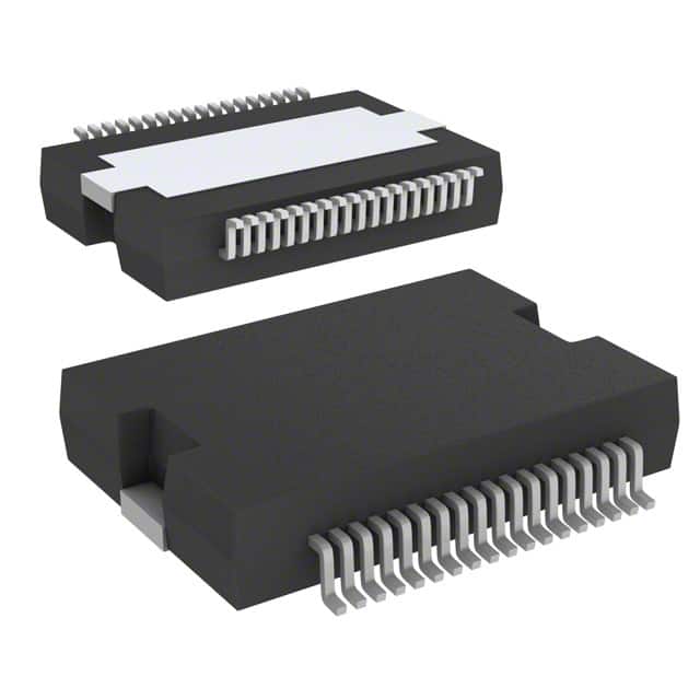
- Part No.:
- L9954
- Manufacturer:
- STMicroelectronics
- Category:
- Power Management - Specialized
- Package:
- PowerSO-36 Exposed Bottom Pad
- Datasheet:
-
 L9954.pdf
- Description:
- IC DVR DOOR ACTUATOR POWERSO-36
- Quantity:
- Payment:

- Shipping:

Inventory:1,194
Please send an inquiry. Send us your inquiry, and we will respond immediately.
Product details
Overview
L9954 from STMicroelectronics is an automotive-grade, SPI-controlled door actuator driver IC integrating three half-bridge outputs (±1.5 A, RON = 800 mΩ), one 6 A high-side driver (RON = 100 mΩ), and two additional 1.5 A high-side drivers (RON = 800 mΩ), designed for mirror axis control, defroster heating, and 10 W bulb driving in vehicle door modules.
For engineers reviewing the L9954 datasheet, L9954 pinout, L9954 application, or L9954 equivalent, this device supports PWM-controlled bidirectional motor drive, real-time current monitoring (OUT1/4/5/6), open-load and overload diagnostics, programmable softstart, and reverse-polarity protection via external MOSFET driven by its charge pump output.
Technical Context
The L9954 implements a microcontroller-driven architecture with a 24-bit SPI interface for command input and status readback, enabling precise control of six independent outputs (three half-bridges + three high-side drivers) with configurable fault reporting. All outputs feature integrated overtemperature, short-circuit, and open-load protection.
Its dual-supply design separates VS (7–28 V battery rail) from VCC (4.5–5.3 V logic supply), and includes dedicated diagnostic functions: current monitor scaling (1:10,000), programmable softstart for inrush current management (>6 A), and cross-current protection with 200–400 µs dead-time enforcement between high- and low-side switching.
Key Specifications
| Parameter | Value and Actual Design Meaning |
|---|---|
| Output Configuration | Three half-bridges (OUT1–OUT3) + three high-side drivers (OUT4–OUT6) |
| Max Output Current | ±3 A sink/source per half-bridge; −6 A source for OUT6; −3 A source for OUT4/OUT5 |
| RON (Typ) | 800 mΩ (half-bridges & OUT4/OUT5); 100 mΩ (OUT6) |
| Standby Current | <6 µA at Tj ≤ 85 °C - enables ultra-low-power vehicle sleep-mode compliance |
| Diagnostic Coverage | Open-load detection (15–60 mA threshold), overload detection, overtemperature warning (130 °C) and shutdown (170 °C) |
| SPI Interface | 24-bit serial command/status register with CSN/CLK/DI/DO; supports real-time fault reporting and configuration |
| Charge Pump Output | VCP = VS + 6 to VS + 13 V - drives external N-MOSFET for reverse-polarity protection |
Pinout & Package
Package: PowerSO-36 (exposed thermal pad, RoHS-compliant, ECOPACK®). Designed for high-power automotive PCB mounting with multiple GND and VS pins for low-impedance current return and supply routing.
| Pin/Terminal | Circuit Role | Design Meaning |
|---|---|---|
| 1, 18, 19, 36 | GND | Reference ground; all four pins must be externally connected to sustain full output current and thermal performance |
| 2, 35 | OUT6 | 6 A high-side driver output; no internal GND-reverse diode; protected against open load and overcurrent |
| 3–5 | OUT1–OUT3 | Half-bridge outputs; each integrates complementary DMOS high-/low-side switches with bulk-drain freewheeling diodes |
| 6, 7, 14, 25, 28, 32 | VS | Main power supply input (7–28 V); six pins required for low-impedance connection to battery rail |
| 8 | DI | SPI data input (CMOS level); receives 24-bit command word LSB-first from MCU |
| 9 | CM/PWM2 | Bidirectional pin: current monitor output (1:10,000 scaling) or secondary PWM input for OUT5 |
| 10 | CSN | Active-low SPI chip select; enables serial communication and enters test mode when held low during power-up |
| 11 | DO | SPI data output (tri-state); delivers 24-bit status register on CSN low; high-impedance otherwise |
| 12 | VCC | Logic supply (4.5–5.3 V); requires local ceramic decoupling to GND |
| 13 | CLK | SPI clock input (CMOS level); controls internal shift register timing |
| 26 | CP | Charge pump output; provides boosted gate drive (VS+6 to VS+13 V) for external reverse-polarity N-MOSFET |
| 27 | PWM1 | Hardware PWM input controlling OUT1–OUT4 and OUT6; bypasses SPI for time-critical actuation |
| 31, 33 | OUT4, OUT5 | 1.5 A high-side drivers; intended for resistive loads (e.g., mirror defroster, 10 W bulbs); open-load protected |
Key Features
| Feature | Design Value |
|---|---|
| Programmable Softstart | Configurable ramp rate for inductive loads (e.g., mirror motors) to limit inrush current >6 A without triggering overcurrent fault |
| Current Monitor Outputs | Analog current sense on OUT1, OUT4, OUT5, and OUT6 with 1:10,000 scaling and ±8% accuracy - enables closed-loop current regulation |
| Reverse Polarity Protection Support | Integrated charge pump (VCP = VS+6 to VS+13 V) drives external N-channel MOSFET gate - eliminates need for bulky series P-MOSFET |
| Dual Supply Architecture | Independent VS (7–28 V) and VCC (4.5–5.3 V) rails - isolates noisy battery transients from logic circuitry and improves EMC robustness |
| Comprehensive Diagnostics | Per-output open-load detection (15–60 mA), overload flagging, junction temperature warning (130 °C), and thermal shutdown (170 °C) |
Applications
| Mirror Axis Control | Mirror Defroster Drive |
|---|---|
|
Use Scenario: Bidirectional positioning of side-view mirrors using DC motors. IC Role / Device Role / Timing Role: Half-bridge driver (OUT1–OUT3) delivers ±1.5 A with PWM-controlled direction and braking; SPI reports stall or open-circuit faults. Use Value: Enables precise, noise-immune motor control with real-time diagnostics - reduces ECU software overhead and improves ASIL-B functional safety compliance. |
Use Scenario: Heating element activation in rearview/side mirrors under low-temperature conditions. IC Role / Device Role / Timing Role: High-side driver (OUT6) supplies up to 6 A to resistive defroster trace; programmable softstart prevents cold-resistance surge. Use Value: Eliminates inrush-triggered fuse blowing and supports rapid thermal response while maintaining diagnostic visibility. |
| Door Light Control | Lock/Folder Actuation |
|
Use Scenario: Switching 10 W incandescent or LED bulbs for interior door lighting. IC Role / Device Role / Timing Role: High-side drivers (OUT4/OUT5) deliver −1.5 A with open-load detection - confirms bulb integrity before illumination. Use Value: Prevents false "bulb-out" warnings and enables predictive maintenance via continuous filament health monitoring. |
Use Scenario: Driving solenoid-based door lock actuators or folder mechanisms. IC Role / Device Role / Timing Role: Half-bridge (OUT1–OUT3) provides controlled energy delivery with cross-current protection and thermal foldback. Use Value: Ensures reliable mechanical engagement under voltage sag (e.g., cranking) and avoids coil burnout during extended hold states. |
Equivalent & Alternatives
The following parts are listed as comparable options for similar door actuator driver applications.
| Alternative Part | Technical Difference | Application Difference | Selection Advice |
|---|---|---|---|
| TLE9201SE | Single half-bridge (2.8 A), no integrated current monitor; SPI interface limited to status only (no command write) | Lacks multi-output integration - requires 3× TLE9201SE + external logic for same functionality as L9954 | Use only when system-level consolidation is not required and cost-per-channel is prioritized over board space and diagnostic depth. |
| BD37102EFV | Three half-bridges (1.2 A), no high-side drivers; analog current sense only on one channel; no charge pump | Cannot drive mirror defroster or bulbs directly - needs external high-side switches and reverse-polarity circuitry | Select if application uses only motor control and external components are acceptable for non-motor loads. |
Compared with TLE9201SE and BD37102EFV, the L9954 provides unified control of mixed motor/resistive loads in a single package, with deeper diagnostics (per-output open-load, current monitor on four channels), integrated reverse-polarity support, and higher peak current capability - reducing BOM count and improving functional safety coverage.
Availability
L9954 is available at Aetrix Electronics and suitable for automotive door module design, mirror actuation systems, and body control unit (BCU) subassemblies requiring stable component supply across production lifecycles.
Supply support for L9954 includes scheduled delivery planning, volume procurement assistance, BOM continuity management, traceable sourcing, and lifecycle availability coordination for OEM customers, industrial embedded developers, connected-device designers, and electronics production programs.
Manufacturer
STMicroelectronics is a global semiconductor leader specializing in automotive, industrial, and power management ICs, with broad portfolio certification to AEC-Q100 and ISO 26262 standards.
The L9954 belongs to ST's automotive smart-power driver family, engineered specifically for body electronics applications demanding high integration, robust diagnostics, and ASIL-ready fault handling in harsh vehicle environments.
FAQ
What is the maximum allowable junction temperature for continuous operation?
The L9954 specifies an operating junction temperature range of −40 °C to +150 °C. Thermal shutdown activates at +170 °C (rising), with hysteresis of +5 K, returning to active mode at +150 °C (falling). Sustained operation above +150 °C risks derating and reduced reliability; thermal design must maintain Tj ≤ 130 °C to avoid temperature warning flag assertion.
Can OUT4 and OUT5 drive 12 V, 10 W incandescent bulbs directly?
Yes - OUT4 and OUT5 are rated for −3 A source current at VS = 13.5 V and Tj = 25 °C, well above the ~0.83 A required for a 10 W bulb at 12 V. Their 800 mΩ typical RON yields <1 V drop at full load, ensuring >11 V delivered to the filament. Open-load diagnostics confirm bulb integrity during startup and runtime.
How does the charge pump (CP pin) interface with external reverse-polarity protection?
The CP pin delivers a boosted voltage (VS + 6 to VS + 13 V) to drive the gate of an external N-channel MOSFET placed between battery and VS. This configuration replaces less efficient P-MOSFET solutions, reducing conduction loss and footprint. The CP output sustains ≥95 µA at VCP = VS + 10 V, sufficient for standard automotive N-MOSFET gate capacitance.
Is PWM1 compatible with standard 5 V MCU GPIO outputs?
Yes - PWM1 accepts CMOS logic levels referenced to VCC (4.5–5.3 V). A 5 V-tolerant MCU GPIO can directly drive it without level-shifting. The input supports standard PWM frequencies up to 20 kHz, and its signal path bypasses the SPI interface to enable deterministic, low-latency actuation for time-critical functions like emergency lock engagement.
L9954 Specifications
- Product attributes
- Attribute value
- Manufacturer:
- STMicroelectronics
- Series:
- -
- Package/Case:
- PowerSO-36 Exposed Bottom Pad
- Packaging:
- Tube
- Product Status:
- Obsolete
- Applications:
- -
- Current - Supply:
- 7mA
- Voltage - Supply:
- 7V ~ 28V
- Operating Temperature:
- -40°C ~ 150°C
- Grade:
- Automotive
- Qualification:
- -
- Mounting Type:
- Surface Mount
- Supplier Device Package:
- PowerSO-36
L9954 FAQ
1.How can I place an order for L9954 through Aetrix?
Please submit a Request for Quotation (RFQ) for L9954 on Aetrix. Our sales agent will provide a competitive quotation and guide you through the order confirmation once you accept the terms.
2.Are the price and stock information for L9954 reliable?
The price and inventory of L9954 are updated periodically and may fluctuate due to market conditions. Stock and pricing data are typically refreshed every 24 hours. Quotation validity for L9954 is usually 5 days.
3.What payment methods are accepted for L9954?
We accept Wire Transfer, PayPal, Credit Card, Western Union, MoneyGram, and Escrow for L9954 transactions.
Note: Certain payment methods may incur a processing fee.
4.How is shipping managed for L9954?
L9954 orders can be shipped via leading logistics carriers, including DHL, UPS, FedEx, TNT, or Registered Mail.
Once your L9954 order is processed, you will receive an email with the shipment details and tracking number.
Note: Tracking information may take up to 24 hours to appear. Express delivery typically takes 3–5 business days.
5.How can I obtain technical support or documentation for L9954?
For technical support, including L9954 datasheets, pinout diagrams, or application guidance, please contact our engineering support team. They can provide detailed documentation and assistance for your L9954 requirements.
6.How does Aetrix verify that L9954 is sourced from the original manufacturer or authorized distributors?
All L9954 products on Aetrix are procured from qualified distributors and authorized channels. Our dedicated quality assurance team conducts strict verification, including traceability checks and, if necessary, third-party testing. This ensures that L9954 meets industry standards.
7.What is the process for return or replacement of L9954?
All L9954 units undergo pre-shipment inspection (PSI). If there is an issue with L9954, returns or replacements are accepted under the following conditions:
1.Quantity discrepancies, incorrect items, or visible external defects (such as breakage or corrosion), acknowledged by Aetrix.
2.The issue is reported within 90 days of delivery.
3.The L9954 part is unused and in its original packaging.
Return procedure for L9954:
1.Submit a request within 90 days.
2.Obtain a Return Material Authorization (RMA) from Aetrix.
L9954 Tags

-
TPS2511DGNR
Texas Instruments

-
UTC2000/MG
Microchip Technology

-
TUSB320HAIRWBR
Texas Instruments

-
TPS61252DSGR
Texas Instruments

-
PI5USB30216CXUAEX
Diodes Incorporated

-
SN6501DBVR
Texas Instruments

-
CYPD3177-24LQXQT
Infineon Technologies
-
SN6501QDBVRQ1
Texas Instruments

-
STUSB1600AQTR
STMicroelectronics

-
SN6505BDBVR
Texas Instruments
-
SN6501DBVT
Texas Instruments

-
TPS65150PWPR
Texas Instruments
Tech Hub

A practical engineering and sourcing framework covering lifecycle verification, lifetime-buy calculations, replacement qualification, supplier checks and counterfeit-risk controls.

TTL and CMOS logic families differ in thresholds, loading, output drive, power and timing. This engineering guide compares 74HC and 74HCT, calculates noise margins and checks 3.3 V/5 V compatibility.

A practical engineering guide to 3.3V and 5V logic compatibility, input thresholds, resistor dividers, translator ICs, MOSFET level shifting, I2C pull-ups, timing limits and power-sequencing risks.

The 74HC595 uses push-pull logic outputs, while the TPIC6B595 uses 50 V open-drain DMOS sinks for higher-power loads. This guide compares timing, current limits, 3.3 V interfacing, load wiring, thermal…

The 74HC595 converts serial data into eight stable parallel outputs. This guide covers pin functions, shift and storage timing, OE and MR behavior, drive-current limits, cascading, voltage compatibilit…

A technical comparison of level-sensitive latches and edge-triggered flip-flops, covering timing windows, setup and hold limits, master–slave operation, time borrowing, race-through, HDL inference and…

A D latch stores one bit while Enable controls when data can pass. This reference covers gate-level operation, truth tables, transparency, setup and hold timing, LE versus OE, common ICs and practical …

An SR latch stores one bit through cross-coupled feedback. This engineering reference covers NOR and NAND implementations, truth tables, forbidden-state recovery, gated operation, switch debouncing, fa…

Latch circuits retain one bit through feedback. This technical reference covers SR and D latches, truth tables, transparency, timing limits, latch-versus-flip-flop behavior, applications and common log…

An engineering guide to LED driver operation, constant-current and constant-voltage outputs, linear and switching topologies, dimming, IC selection, calculations, replacement compatibility, and fault c…


